 | –≠–ª–µ–∫—Ç—Ä–æ–Ω–Ω—ã–π –∫–æ–º–ø–æ–Ω–µ–Ω—Ç: BF992R | –°–∫–∞—á–∞—Ç—å:  PDF PDF  ZIP ZIP |
Document Outline
- APPLICATIONS
- DESCRIPTION
- PINNING
- QUICK REFERENCE DATA
- LIMITING VALUES
- THERMAL CHARACTERISTICS
- STATIC CHARACTERISTICS
- DYNAMIC CHARACTERISTICS
- PACKAGE OUTLINE
- DEFINITIONS
- LIFE SUPPORT APPLICATIONS
DATA SHEET
Product specification
Supersedes data of 1996 Jul 30
1999 Aug 11
DISCRETE SEMICONDUCTORS
BF992
Silicon N-channel dual gate
MOS-FET
M3D071
1999 Aug 11
2
Philips Semiconductors
Product specification
Silicon N-channel dual gate MOS-FET
BF992
APPLICATIONS
∑
VHF applications such as VHF television tuners and FM
tuners with 12 V supply voltage. The device is also
suitable for use in professional communications
equipment.
DESCRIPTION
Depletion type field-effect transistor in a plastic
micro-miniature SOT143B package with source and
substrate interconnected.
The transistor is protected against excessive input voltage
surges by integrated back-to-back diodes between gates
and source.
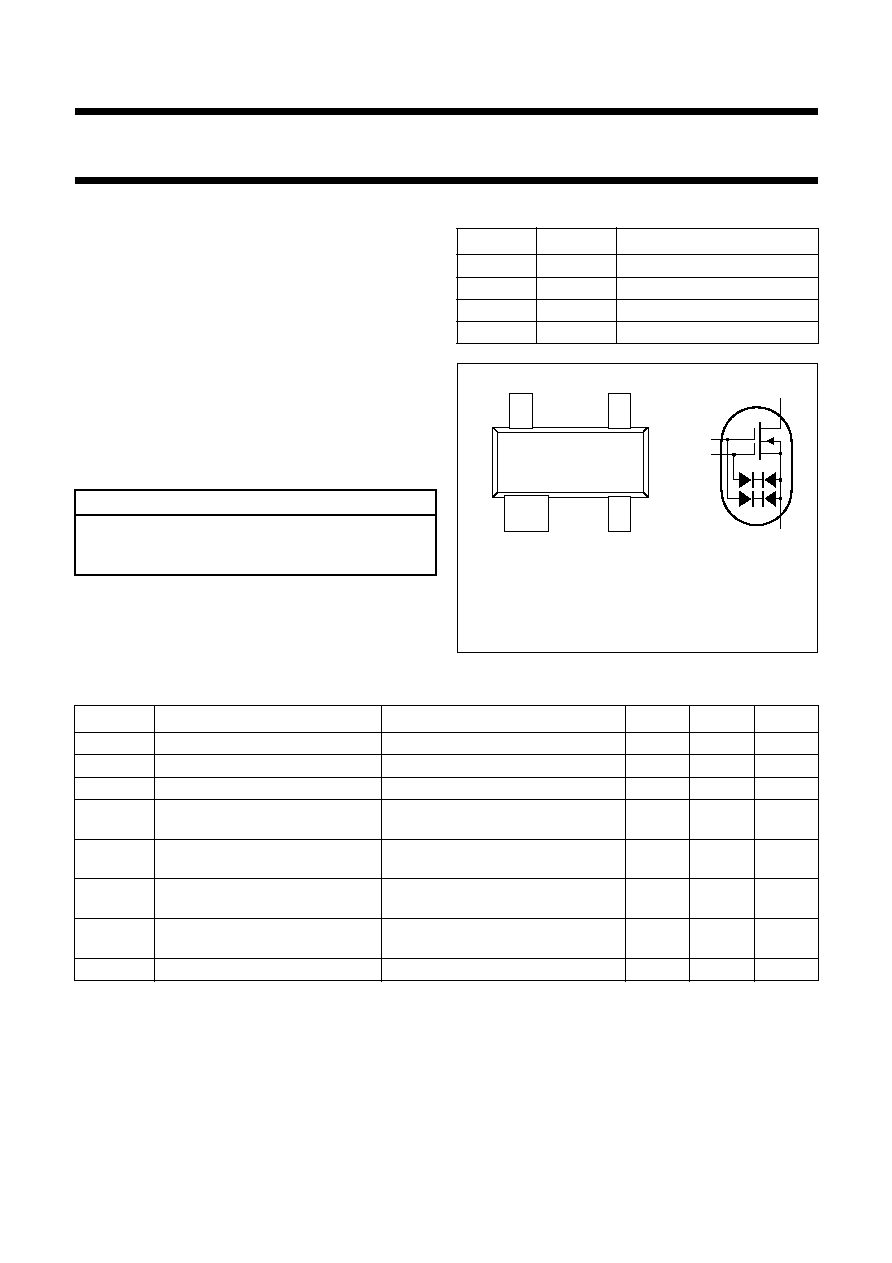
PINNING
CAUTION
The device is supplied in an antistatic package.
The gate-source input must be protected against static
discharge during transport or handling.
PIN
SYMBOL
DESCRIPTION
1
s, b
source
2
d
drain
3
g
2
gate 2
4
g
1
gate 1
Fig.1
Simplified outline (SOT143B) and symbol.
Marking code: M92.
handbook, halfpage
s,b
d
g
1
g
2
4
3
2
1
Top view
MAM039
QUICK REFERENCE DATA
SYMBOL
PARAMETER
CONDITIONS
TYP.
MAX.
UNIT
V
DS
drain-source voltage (DC)
-
20
V
I
D
drain current (DC)
-
40
mA
P
tot
total power dissipation
T
amb
= 60
∞
C
-
200
mW
Y
fs
forward transfer admittance
f = 1 kHz; I
D
= 15 mA; V
DS
= 10 V;
V
G2-S
= 4 V
25
-
mS
C
ig1-s
input capacitance at gate 1
f = 1 MHz; I
D
= 15 mA; V
DS
= 10 V;
V
G2-S
= 4 V
4
-
pF
C
rs
reverse transfer capacitance
f = 1 MHz; I
D
= 15 mA; V
DS
= 10 V;
V
G2-S
= 4 V
30
-
fF
F
noise figure
G
S
= 2 mS; I
D
= 15 mA; V
DS
= 10 V;
V
G2-S
= 4 V; f = 200 MHz
1.2
-
dB
T
j
operating junction temperature
-
150
∞
C
1999 Aug 11
3
Philips Semiconductors
Product specification
Silicon N-channel dual gate MOS-FET
BF992
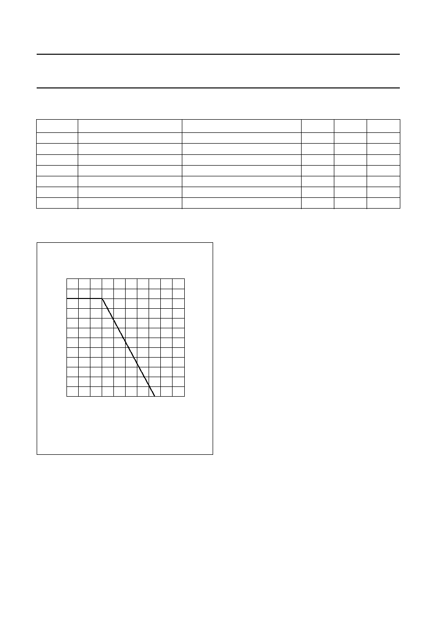
LIMITING VALUES
In accordance with the Absolute Maximum Rating System (IEC 134).
Note
1. Device mounted on a ceramic substrate, 8 mm
◊
10 mm
◊
0.7 mm.
SYMBOL
PARAMETER
CONDITIONS
MIN.
MAX.
UNIT
V
DS
drain-source voltage
-
20
V
I
D
drain current
-
40
mA
I
G1
gate 1 current
-
±
10
mA
I
G2
gate 2 current
-
±
10
mA
P
tot
total power dissipation
T
amb
60
∞
C; see Fig.2; note 1
-
200
mW
T
stg
storage temperature
-
65
+150
∞
C
T
j
operating junction temperature
-
150
∞
C
Fig.2 Power derating curves.
handbook, halfpage
0
100
0
200
100
200
(mW)
Ptot max
MBL033
Tamb ( C)
o
1999 Aug 11
4
Philips Semiconductors
Product specification
Silicon N-channel dual gate MOS-FET
BF992
THERMAL CHARACTERISTICS
Note
1. Device mounted on a ceramic substrate, 8 mm
◊
10 mm
◊
0.7 mm.
STATIC CHARACTERISTICS
T
j
= 25
∞
C unless otherwise specified.
DYNAMIC CHARACTERISTICS
Common source; T
amb
= 25
∞
C; V
DS
= 10 V; V
G2-S
= 4 V; I
D
= 15 mA; unless otherwise specified.
SYMBOL
PARAMETER
CONDITIONS
VALUE
UNIT
R
th j-a
thermal resistance from junction to ambient in free air
note 1
460
K/W
SYMBOL
PARAMETER
CONDITIONS
MIN.
MAX.
UNIT
±
V
(BR)G1-SS
gate 1-source breakdown voltage
V
G2-S
= V
DS
= 0; I
G1-SS
=
±
10 mA
8
20
V
±
V
(BR)G2-SS
gate 2-source breakdown voltage
V
G1-S
= V
DS
= 0; I
G2-SS
=
±
10 mA
8
20
V
-
V
(P)G1-S
gate 1-source cut-off voltage
V
G2-S
= 4 V; V
DS
= 10 V; I
D
= 20
µ
A
0.2
1.3
V
-
V
(P)G2-S
gate 2-source cut-off voltage
V
G1-S
= 0; V
DS
= 10 V; I
D
= 20
µ
A
0.2
1.1
V
±
I
G1-SS
gate 1 cut-off current
V
G2-S
= V
DS
= 0; V
G1-S
=
±
7 V
-
25
nA
±
I
G2-SS
gate 2 cut-off current
V
G1-S
= V
DS
= 0; V
G2-S
=
±
7 V
-
25
nA
SYMBOL
PARAMETER
CONDITIONS
MIN.
TYP.
MAX.
UNIT
y
fs
forward transfer admittance
20
25
-
mS
C
ig1-s
input capacitance at gate 1
f = 1 MHz
-
4
-
pF
C
ig2-s
input capacitance at gate 2
f = 1 MHz
-
1.7
-
pF
C
os
output capacitance
f = 1 MHz
-
2
-
pF
C
rs
reverse transfer capacitance
f = 1 MHz
-
30
40
fF
F
noise figure
f = 200 MHz; G
S
= 2 mS
-
1.2
-
dB
1999 Aug 11
5
Philips Semiconductors
Product specification
Silicon N-channel dual gate MOS-FET
BF992
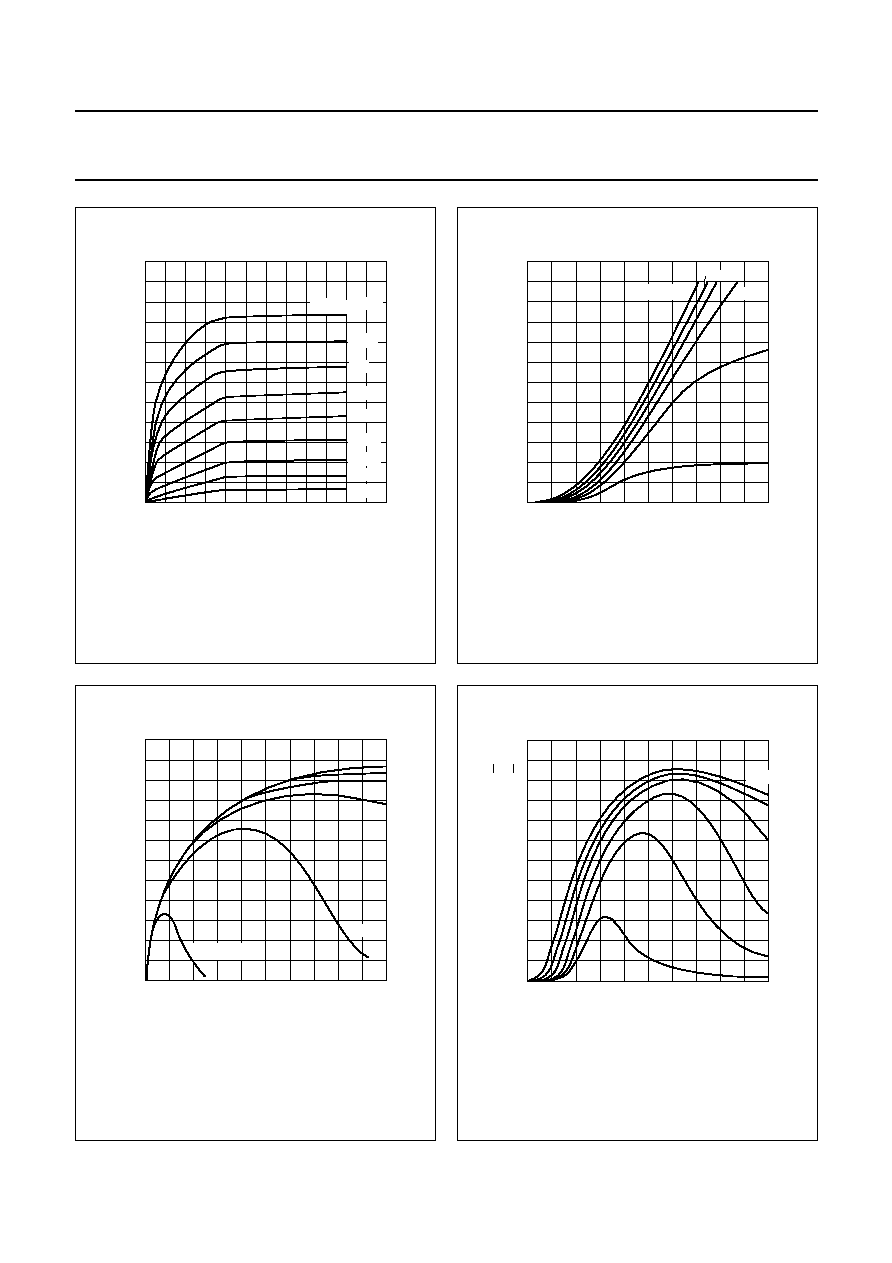
Fig.3 Output characteristics; typical values.
handbook, halfpage
12
MGE797
0
10
24
0
8
16
4
12
20
2
4
6
8
VDS (V)
ID
(mA)
0.1 V
0 V
-
0.5 V
-
0.6 V
-
0.4 V
-
0.3 V
-
0.2 V
-
0.1 V
VG1-S = 0.2 V
V
G2-S
= 4 V; T
j
= 25
∞
C.
Fig.4 Transfer characteristics; typical values.
handbook, halfpage
-
1
1
30
0
10
20
MGE799
0
4 V
3 V
2 V
1 V
0 V
VG2-S = 5 V
VG1-S (V)
ID
(mA)
V
DS
= 10 V; T
j
= 25
∞
C.
Fig.5
Forward transfer admittance as a function
of drain current; typical values.
handbook, halfpage
0
20
30
0
10
20
MGE798
10
ID (mA)
1 V
5 V
2 V
3 V
4 V
VG2-S = 0 V
|yfs|
(mS)
V
DS
= 10 V; T
j
= 25
∞
C.
Fig.6
Forward transfer admittance as a function
of gate 1-source voltage; typical values.
handbook, halfpage
-
1
1
30
0
10
20
MGE800
0
Yfs
(mS)
4 V
5 V
3 V
2 V
1 V
0 V
VG2-S =
VG1-S (V)
V
DS
= 10 V; T
j
= 25
∞
C.