 | –≠–ª–µ–∫—Ç—Ä–æ–Ω–Ω—ã–π –∫–æ–º–ø–æ–Ω–µ–Ω—Ç: BFG10W | –°–∫–∞—á–∞—Ç—å:  PDF PDF  ZIP ZIP |

DATA SHEET
Product specification
File under Discrete Semiconductors, SC14
1995 Sep 22
DISCRETE SEMICONDUCTORS
BFG10W/X
UHF power transistor
1995 Sep 22
2
Philips Semiconductors
Product specification
UHF power transistor
BFG10W/X
FEATURES
∑
High efficiency
∑
Small size discrete power amplifier
∑
900 MHz and 1.9 GHz operating
areas
∑
Gold metallization ensures
excellent reliability.
APPLICATIONS
∑
Common emitter class-AB
operation in hand-held radio
equipment up to 1.9 GHz.
DESCRIPTION
NPN silicon planar epitaxial transistor
encapsulated in a plastic, 4-pin
dual-emitter SOT343 package.
PINNING
PIN
DESCRIPTION
1
collector
2
emitter
3
base
4
emitter
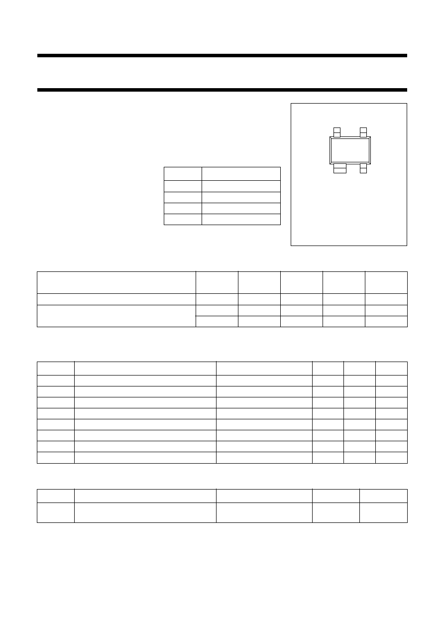
Fig.1 SOT343.
Marking code: T5.
fpage
Top view
MBK523
2
1
3
4
QUICK REFERENCE DATA
RF performance at T
amb
= 25
∞
C in a common-emitter test circuit.
LIMITING VALUES
In accordance with the Absolute Maximum Rating System (IEC 134).
THERMAL CHARACTERISTICS
Note to the Limiting values and Thermal characteristics
1. T
s
is the temperature at the soldering point of the collector pin.
MODE OF OPERATION
f
(GHz)
V
CE
(V)
P
L
(mW)
G
p
(dB)
c
(%)
Pulsed, class-AB, duty cycle: < 1 : 2; t
p
= 10 ms
1.9
3.6
200
5
50
Pulsed, class-AB, duty cycle: < 1 : 8; t
p
= 4.6 ms
0.9
6
650
10
50
0.9
6
360
12.5
50
SYMBOL
PARAMETER
CONDITIONS
MIN.
MAX.
UNIT
V
CBO
collector-base voltage
open emitter
-
20
V
V
CEO
collector-emitter voltage
open base
-
10
V
V
EBO
emitter-base voltage
open collector
-
2.5
V
I
C
collector current (DC)
-
250
mA
I
C(AV)
average collector current
-
250
mA
P
tot
total power dissipation
up to T
s
= 102
∞
C; note 1
-
400
mW
T
stg
storage temperature
-
65
+150
∞
C
T
j
junction temperature
-
175
∞
C
SYMBOL
PARAMETER
CONDITIONS
VALUE
UNIT
R
th j-s
thermal resistance from junction to
soldering point
up to T
s
= 102
∞
C; note 1;
P
tot
= 400 mW
180
K/W
1995 Sep 22
3
Philips Semiconductors
Product specification
UHF power transistor
BFG10W/X
CHARACTERISTICS
T
j
= 25
∞
C (unless otherwise specified).
SYMBOL
PARAMETER
CONDITIONS
MIN.
MAX.
UNIT
V
(BR)CBO
collector-base breakdown voltage
open emitter; I
C
= 0.1 mA
20
-
V
V
(BR)CEO
collector-emitter breakdown voltage
open base; I
C
= 5 mA
10
-
V
V
(BR)EBO
emitter-base breakdown voltage
open collector; I
E
= 0.1 mA
2.5
-
V
I
CES
collector cut-off current
V
CE
= 6 V; V
BE
= 0
-
100
µ
A
h
FE
DC current gain
I
C
= 50 mA; V
CE
= 5 V
25
-
C
c
collector capacitance
I
E
= i
e
= 0; V
CB
= 6 V; f = 1 MHz
-
3
pF
C
re
feedback capacitance
I
C
= 0; V
CE
= 6 V; f = 1 MHz
-
2
pF
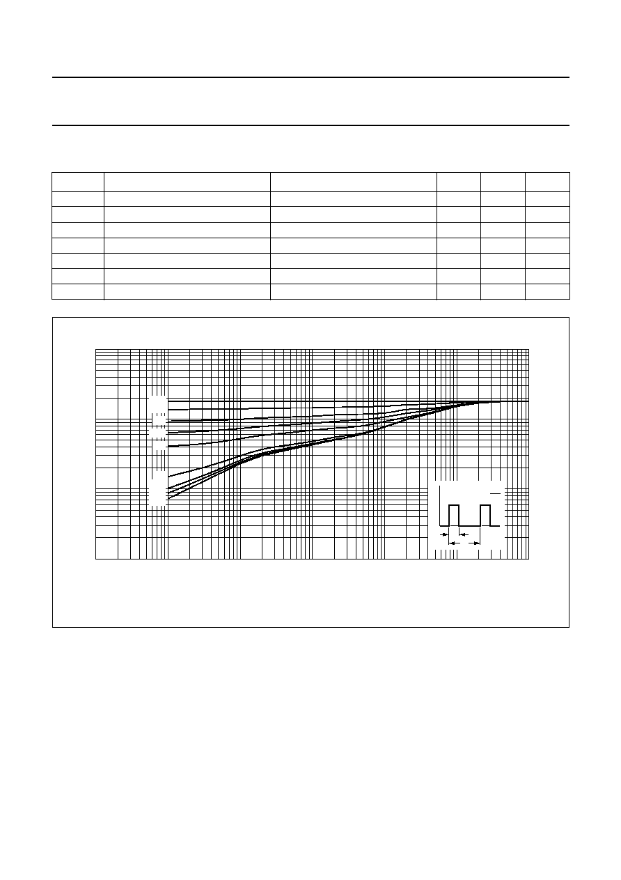
Fig.2 Transient thermal impedance from junction to soldering point as a function of pulse time; typical values.
handbook, full pagewidth
MBG431
10
-
5
10
-
6
10
-
4
10
-
3
10
-
2
10
-
1
1
10
3
10
2
10
1
Zth j-a
(K/W)
tp (s)
= 1
0.75
0.5
0.33
0.2
0.1
0.05
0.02
0.01
t p
T
P
t
t p
T
=
1995 Sep 22
4
Philips Semiconductors
Product specification
UHF power transistor
BFG10W/X
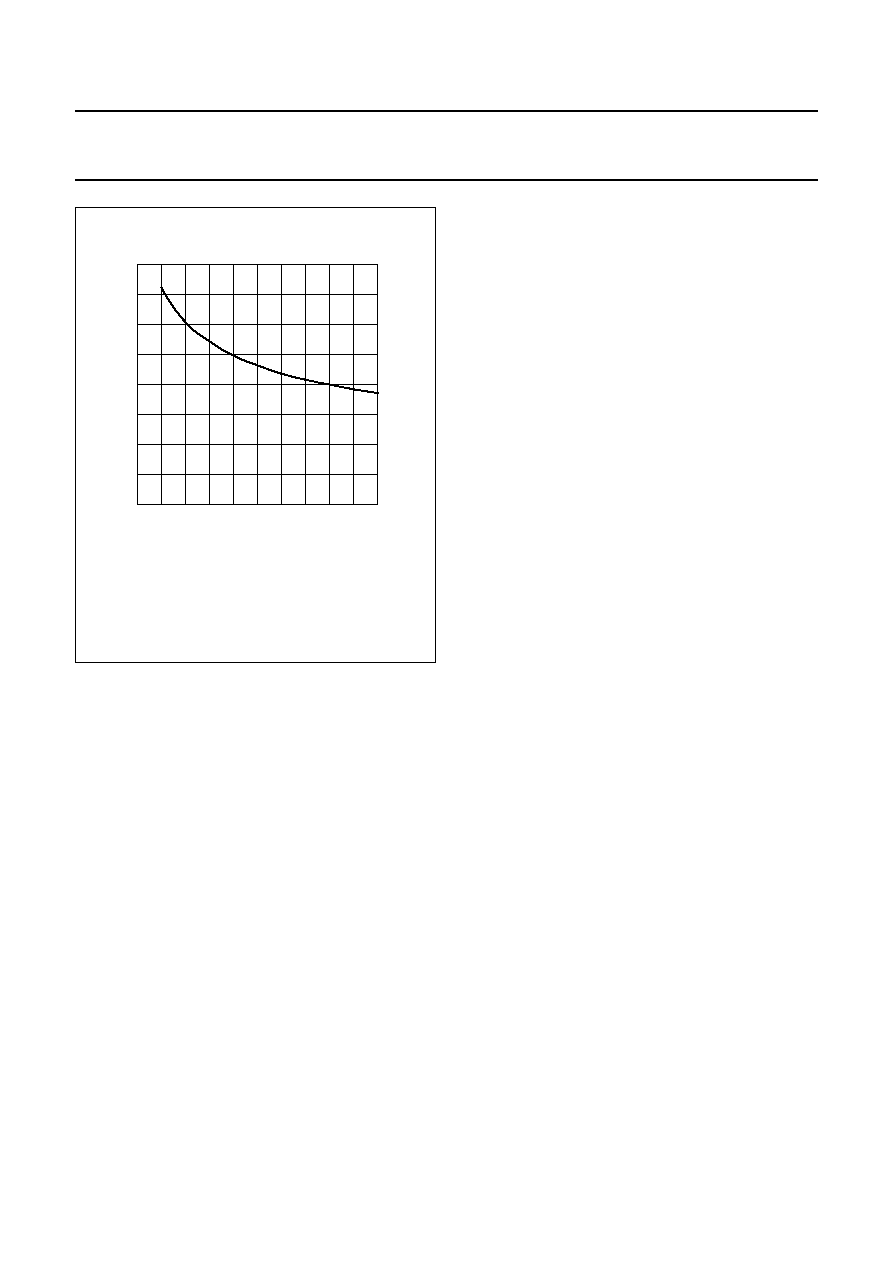
Fig.3
Collector capacitance as a function of
collector-base voltage.
handbook, halfpage
MLC819
0
10
4
8
2.0
0
1.5
6
1.0
0.5
C c
(pF)
VCB (V)
2
1995 Sep 22
5
Philips Semiconductors
Product specification
UHF power transistor
BFG10W/X
APPLICATION INFORMATION
RF performance at T
amb
= 25
∞
C in a common-emitter test circuit.
Ruggedness in class-AB operation
The BFG10W/X is capable of withstanding a load mismatch corresponding to VSWR = 6 : 1 through all phases under
pulsed conditions up to a supply voltage of 8.6 V under the conditions: 900 MHz; 650 mW; t
p
= 4.6 ms; duty cycle of 1 : 8
and up to a supply voltage of 5.5 V under the conditions: 1.9 GHz; 200 mW; t
p
= 10 ms; duty cycle of 1 : 2.
MODE OF OPERATION
f
(GHz)
V
CE
(V)
P
L
(mW)
G
p
(dB)
c
(%)
Pulsed, class-AB, duty cycle: < 1 : 2; t
p
= 10 ms
1.9
3.6
200
5; typ. 7
50; typ. 60
Pulsed, class-AB, duty cycle: < 1 : 8; t
p
= 5 ms
0.9
6
650
10
50
0.9
6
360
12.5
50
Pulsed, class-AB operation.
V
CE
= 3.6 V; f = 1.9 GHz; duty cycle < 1 : 2.
Circuit optimized for P
L
= 200 mW.
Fig.4
Power gain and efficiency as functions
of load power; typical values.
handbook, halfpage
0
500
10
0
2
MLC820
4
6
8
100
0
20
40
60
80
100
200
300
400
G p
G p
(dB)
P (mW)
L
c
(%)
c
Fig.5
Power gain and efficiency as functions
of load power; typical values.
Pulsed, class-AB operation.
V
CE
= 6 V; f = 900 MHz; duty cycle < 1 : 8.
Circuit optimized for P
L
= 600 mW.
handbook, halfpage
0.3
16
0
MBG194
4
8
12
80
20
20
40
60
0.5
0.7
0.9
1.1
G p
G p
(dB)
P (mW)
L
c
(%)
c