 | –≠–ª–µ–∫—Ç—Ä–æ–Ω–Ω—ã–π –∫–æ–º–ø–æ–Ω–µ–Ω—Ç: BFG11W/X | –°–∫–∞—á–∞—Ç—å:  PDF PDF  ZIP ZIP |
Document Outline
- FEATURES
- APPLICATIONS
- DESCRIPTION
- PINNING - SOT343
- QUICK REFERENCE DATA
- LIMITING VALUES
- THERMAL CHARACTERISTICS
- CHARACTERISTICS
- APPLICATION INFORMATION
- Ruggedness in class-AB operation
- List of components used in test circuit
- PACKAGE OUTLINE
- DEFINITIONS
- LIFE SUPPORT APPLICATIONS

DATA SHEET
Product specification
Supersedes data of September 1995
File under Discrete Semiconductors, SC14
1996 Jun 04
DISCRETE SEMICONDUCTORS
BFG11W/X
NPN 2 GHz power transistor
1996 Jun 04
2
Philips Semiconductors
Product specification
NPN 2 GHz power transistor
BFG11W/X
FEATURES
∑
High power gain
∑
High efficiency
∑
Small size discrete power amplifier
∑
1.9 GHz operating area
∑
Gold metallization ensures excellent reliability
∑
Linear and non-linear operation.
APPLICATIONS
∑
Common emitter class-AB operation in handheld radio
equipment at 1.9 GHz such as DECT, PHS.
∑
Driver for DCS 1800.
DESCRIPTION
NPN silicon planar epitaxial transistor encapsulated in a
plastic 4-pin dual-emitter SOT343 package.
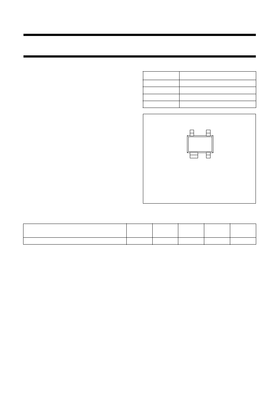
PINNING - SOT343
PIN
DESCRIPTION
1
collector
2
emitter
3
base
4
emitter
Fig.1 Simplified outline.
Marking code: S4
handbook, halfpage
Top view
MBK523
2
1
3
4
QUICK REFERENCE DATA
RF performance at T
s
60
∞
C in a common-emitter test circuit.
MODE OF OPERATION
f
(GHz)
V
CE
(V)
P
L
(mW)
G
p
(dB)
c
(%)
Pulsed, class-AB,
< 1 : 2; t
p
= 5 ms
1.9
3.6
400
6
60
1996 Jun 04
3
Philips Semiconductors
Product specification
NPN 2 GHz power transistor
BFG11W/X
LIMITING VALUES
In accordance with the Absolute Maximum Rating System (IEC 134).
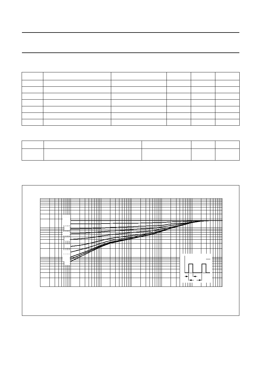
THERMAL CHARACTERISTICS
Note to the Limiting values and Thermal characteristics
1. T
s
is the temperature at the soldering point of the collector tab.
SYMBOL
PARAMETER
CONDITIONS
MIN.
MAX.
UNIT
V
CBO
collector-base voltage
open emitter
-
20
V
V
CEO
collector-emitter voltage
open base
-
8
V
V
EBO
emitter-base voltage
open collector
-
2.5
V
I
C
collector current (DC)
-
500
mA
P
tot
total power dissipation
up to T
s
= 60
∞
C; note 1
-
760
mW
T
stg
storage temperature
-
65
+150
∞
C
T
j
junction temperature
-
175
∞
C
SYMBOL
PARAMETER
CONDITIONS
VALUE
UNIT
R
th j-s
thermal resistance from junction to soldering point
up to T
s
= 60
∞
C;
P
tot
= 760 mW; note 1
150
K/W
Fig.2 Transient thermal impedance from junction to soldering point as a function of pulse time; typical values.
handbook, full pagewidth
MGD411
10
-
5
10
-
6
10
-
4
10
-
3
10
-
2
10
-
1
1
10
3
10
2
10
1
Zth j-s
(K/W)
tp (s)
=
1
0.75
0.5
0.33
0.2
0.1
0.1
0.05
0.02
0.01
t p
T
P
t
t p
T
=
1996 Jun 04
4
Philips Semiconductors
Product specification
NPN 2 GHz power transistor
BFG11W/X
CHARACTERISTICS
T
j
= 25
∞
C unless otherwise specified.
APPLICATION INFORMATION
RF performance at T
s
60
∞
C in a common-emitter test circuit.
Ruggedness in class-AB operation
The transistors are capable of withstanding a load mismatch corresponding to VSWR = 8 : 1 through all phases, at rated
output power under pulsed conditions at f = 1.9 GHz: t
p
= 1.25 ms,
= 1 : 8 at V
CE
= 7 V and t
p
= 5 ms,
= 1 : 2 at
V
CE
= 4.5 V.
SYMBOL
PARAMETER
CONDITIONS
MIN.
MAX.
UNIT
V
(BR)CBO
collector-base breakdown voltage
I
C
= 0.1 mA; open emitter
20
-
V
V
(BR)CEO
collector-emitter breakdown voltage
I
C
= 10 mA; open base
8
-
V
V
(BR)EBO
emitter-base breakdown voltage
I
E
= 0.1 mA; open collector
2.5
-
V
I
CES
collector cut-off current
V
CE
= 8 V; V
BE
= 0
-
100
µ
A
h
FE
DC current gain
V
CE
= 5 V; I
C
= 100 mA
25
-
C
c
collector capacitance
V
CB
= 3.6 V; I
E
= i
e
= 0; f = 1 MHz
-
5
pF
C
re
feedback capacitance
V
CE
= 3.6 V; I
C
= 0; f = 1 MHz
-
4
pF
MODE OF OPERATION
f
(GHz)
V
CE
(V)
I
CQ
(mA)
P
L
(mW)
G
p
(dB)
c
(%)
Pulsed, class-AB,
< 1 : 2; t
p
= 5 ms
1.9
3.6
1
400
6
60
V
CE
= 3.6 V; V
BE
= 0.65 V; f = 1.9 GHz;
< 1 : 8; t
p
= 1.25 ms.
Fig.3
Power gain and efficiency as functions
of load power; typical values.
handbook, halfpage
0
200
400
800
8
Gp
(dB)
6
2
0
4
90
70
30
10
50
MGD412
600
PL (mW)
C
(%)
C
Gp
V
CE
= 3.6 V; I
c
= 1 mA; f
1
= 1990.0 MHz;
f
2
= 1990.1 MHz;
= 1 : 8; t
p
= 625
µ
s.
Fig.4
Two tone intermodulation distortion
and efficiency as functions of average
output power; typical values.
handbook, halfpage
0
30
0
dim
(dBc)
-
80
-
60
MGD552
-
40
-
20
10
20
Po(av) (dBm)
c
(%)
c
60
80
0
20
40
dim

1996 Jun 04
5
Philips Semiconductors
Product specification
NPN 2 GHz power transistor
BFG11W/X
List of components used in test circuit (see Figs 5 and 6)
Notes
1. American Technical Ceramics (ATC) capacitor, type 100A or other capacitor of the same quality.
2. The striplines are on a double copper-clad printed-circuit board with PTFE fibre-glass dielectric
r
= 6.15;
tan
= 0.0019; thickness = 0.64 mm; copper cladding = 35
µ
m.
3. Or equivalent (V
BE
= 0.65 V at T
amb
= 25
∞
C).
COMPONENT
DESCRIPTION
VALUE
DIMENSIONS
CATALOGUE N0.
C1, C8, C9, C10
multilayer ceramic chip capacitor; note 1
24 pF
C2, C3
multilayer ceramic chip capacitor; note 1
2 pF
C4
multilayer ceramic chip capacitor; note 1
1.2 pF
C5
multilayer ceramic chip capacitor; note 1
0.2 pF
C6, C7,
multilayer ceramic chip capacitor; note 1
1.3 pF
C11, C12, C13
multilayer ceramic chip capacitor; note 1
10 nF
C14, C15
electrolytic capacitor
470
µ
F; 10 V
2222 032 14152
L1
stripline; note 2
length 22.5 mm
width 0.9 mm
L2
stripline; note 2
length 6 mm
width 0.9 mm
L3
stripline; note 2
length 1 mm
width 0.9 mm
L4
stripline; note 2
length 2.5 mm
width 0.9 mm
L5
stripline; note 2
length 4.5 mm
width 0.9 mm
L6
stripline; note 2
length 24.5 mm
width 0.9 mm
L7
stripline; note 2
length 20 mm
width 0.9 mm
L8
stripline; note 2
length 10.5 mm
width 0.9 mm
L9
stripline; note 2
length 4.4 mm
width 0.4 mm
L10
stripline; note 2
length 19.7 mm
width 0.4 mm
L11, L12
RF choke
1
µ
H
4330 030 36301
R1
metal film resistor
78.7
;
0.4 W
R2
metal film resistor
38.3
;
0.4 W
R3
metal film resistor
10
;
0.4 W
T1
bias transistor
BC548; note 3