 | –≠–ª–µ–∫—Ç—Ä–æ–Ω–Ω—ã–π –∫–æ–º–ø–æ–Ω–µ–Ω—Ç: BFG17A | –°–∫–∞—á–∞—Ç—å:  PDF PDF  ZIP ZIP |
Document Outline
- DESCRIPTION
- PINNING
- QUICK REFERENCE DATA
- LIMITING VALUES
- THERMAL CHARACTERISTICS
- CHARACTERISTICS
- PACKAGE OUTLINE
- DEFINITIONS
- LIFE SUPPORT APPLICATIONS

DATA SHEET
Product specification
File under Discrete Semiconductors, SC14
1995 Sep 12
DISCRETE SEMICONDUCTORS
BFG17A
NPN 3 GHz wideband transistor

1995 Sep 12
2
Philips Semiconductors
Product specification
NPN 3 GHz wideband transistor
BFG17A
DESCRIPTION
NPN wideband transistor in a
microminiature plastic SOT143
surface mounting envelope with
double emitter bonding.
It is intended for use in wideband
aerial amplifiers using SMD
technology.
PINNING
PIN
DESCRIPTION
Code: E6
1
collector
2
base
3
emitter
4
emitter
Fig.1 SOT143.
handbook, 2 columns
Top view
MSB014
1
2
3
4
QUICK REFERENCE DATA
LIMITING VALUES
In accordance with the Absolute Maximum System (IEC 134).
Note
1. T
s
is the temperature at the soldering point of the collector tab.
SYMBOL
PARAMETER
CONDITIONS
MIN.
TYP.
MAX.
UNIT
V
CBO
collector-base voltage
open emitter
-
-
25
V
V
CEO
collector-emitter voltage
open base
-
-
15
V
I
C
DC collector current
-
-
50
mA
P
tot
total power dissipation
up to T
s
= 85
∞
C; note 1
-
-
300
mW
h
FE
DC current gain
I
C
= 25 mA; V
CE
= 1 V;
T
amb
= 25
∞
C
20
-
150
f
T
transition frequency
I
C
= 25 mA; V
CE
= 5 V;
f = 500 MHz; T
amb
= 25
∞
C
-
2.8
-
GHz
C
re
feedback capacitance
I
C
= 0; V
CE
= 5 V; f = 1 MHz
-
0.4
-
pF
G
UM
maximum unilateral power gain
I
C
= 15 mA; V
CE
= 10 V;
f = 800 MHz; T
amb
= 25
∞
C
-
15
-
dB
F
noise figure
I
C
= 2 mA; V
CE
= 5 V; f = 800 MHz;
T
amb
= 25
∞
C; Z
S
= 60
; b
s
= opt.
-
2.5
-
dB
SYMBOL
PARAMETER
CONDITIONS
MIN.
MAX.
UNIT
V
CBO
collector-base voltage
open emitter
-
25
V
V
CEO
collector-emitter voltage
open base
-
15
V
V
EBO
emitter-base voltage
open collector
-
2.5
V
I
C
DC collector current
-
50
mA
P
tot
total power dissipation
up to T
s
= 85
∞
C; note 1
-
300
mW
T
stg
storage temperature
-
65
+150
∞
C
T
j
junction temperature
-
175
∞
C

1995 Sep 12
3
Philips Semiconductors
Product specification
NPN 3 GHz wideband transistor
BFG17A
THERMAL CHARACTERISTICS
Note
1. T
s
is the temperature at the soldering point of the collector tab.
CHARACTERISTICS
T
j
= 25
∞
C unless otherwise specified.
Notes
1. G
UM
is the maximum unilateral power gain, assuming S
12
is zero and
.
2. d
im
=
-
60 dB (DIN 45004B, para. 6,3: 3-tone); I
C
= 14 mA; V
CE
= 10 V; Z
L
= 75
.
V
p
= V
o
; f
p
= 795.25 MHz;
V
q
= V
o
-
6 dB; f
q
= 803.25 MHz;
V
r
= V
o
-
6 dB; f
r
= 805.25 MHz;
measured at f
(p+q
-
r)
= 793.25 MHz.
SYMBOL
PARAMETER
CONDITIONS
VALUE
UNIT
R
th j-s
thermal resistance from junction
to soldering point
up to T
s
= 85
∞
C; note 1
290
K/W
SYMBOL
PARAMETER
CONDITIONS
MIN.
TYP.
MAX.
UNIT
I
CBO
collector cut-off current
I
E
= 0; V
CB
= 10 V
-
-
50
nA
h
FE
DC current gain
I
C
= 25 mA; V
CE
= 1 V;
T
amb
= 25
∞
C
20
75
150
f
T
transition frequency
I
C
= 25 mA; V
CE
= 5 V;
f = 500 MHz; T
amb
= 25
∞
C
-
2.8
-
GHz
C
c
collector capacitance
I
E
= 0; V
CB
= 10 V; f = 1 MHz;
T
amb
= 25
∞
C
-
0.7
-
pF
C
e
emitter capacitance
I
C
= 0; V
EB
= 0.5 V; f = 1 MHz
-
1.25
-
pF
C
re
feedback capacitance
I
C
= 0; V
CE
= 5 V; f = 1 MHz
-
0.4
-
pF
G
UM
maximum unilateral power gain
(note 1)
I
C
= 15 mA; V
CE
= 10 V;
f = 800 MHz; T
amb
= 25
∞
C
-
15
-
dB
F
noise figure
I
C
= 2 mA; V
CE
= 5 V; f = 800 MHz;
T
amb
= 25
∞
C; Z
S
= 60
; b
s
= opt.
-
2.5
-
dB
V
o
output voltage
note 2
-
150
-
mV
G
UM
10
s
21
2
1
s
11
2
≠
(
)
1
s
22
2
≠
(
)
------------------------------------------------------------ dB.
log
=
1995 Sep 12
4
Philips Semiconductors
Product specification
NPN 3 GHz wideband transistor
BFG17A
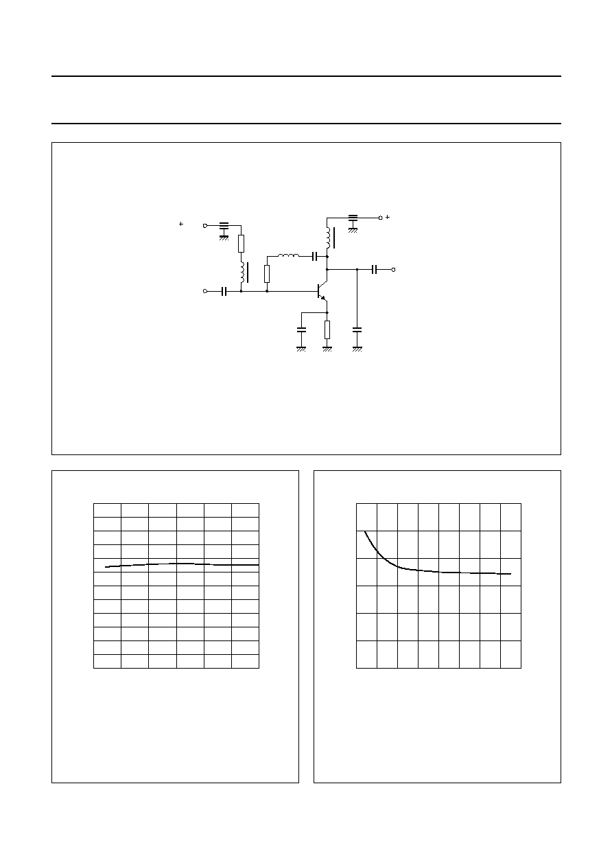
Fig.2 Intermodulation distortion and second order intermodulation distortion MATV test circuit.
(1) L1 = L3 = 5
µ
H Ferroxcube choke.
(2) L2 = 3 turns 0.4 mm copper wire, internal diameter 3 mm, winding pitch 1 mm.
handbook, full pagewidth
MBB251
18
1.5 nF
10 k
L2
L1
1 nF
75
input
270
1 nF
L3
1.5 nF
1 nF
0.68 pF
3.3 pF
DUT
75
output
VCC
VBB
Fig.3
DC current gain as function of collector
current.
V
CE
= 1 V; T
amb
= 25
∞
C.
handbook, halfpage
MBB374
80
120
0
10
20
30
0
I (mA)
C
h FE
40
Fig.4
Collector capacitance as a function of
collector-base voltage.
I
E
= 0; f = 1 MHz; T
amb
= 25
∞
C
handbook, halfpage
MBB370
0
1.2
0.8
0.4
0
4
8
12
16
V (V)
CB
C c
(pF)
1995 Sep 12
5
Philips Semiconductors
Product specification
NPN 3 GHz wideband transistor
BFG17A
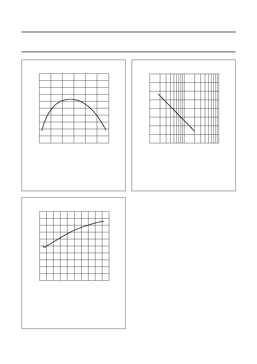
Fig.5
Transition frequency as a function of
collector current.
V
CE
= 5 V; f = 500 MHz; T
amb
= 25
∞
C.
handbook, halfpage
0
10
20
30
4
2
3
MBB373
I (mA)
C
f T
(GHz)
Fig.6
Maximum unilateral power gain as a
function of frequency.
I
C
= 15 mA; V
CE
= 10 V; T
amb
= 25
∞
C.
handbook, halfpage
MBB371
40
0
20
30
10
2
10
3
10
4
10
f (MHz)
G UM
(dB)
Fig.7
Minimum noise figure as a function of
collector current.
V
CE
= 5 V; f = 800 MHz; T
amb
= 25
∞
C; Z
S
= 60
; b
s
= opt.
handbook, halfpage
MBB372
0
5
0
12
4
8
F
(dB)
4
3
2
1
16
20
I (mA)
C