 | –≠–ª–µ–∫—Ç—Ä–æ–Ω–Ω—ã–π –∫–æ–º–ø–æ–Ω–µ–Ω—Ç: BFG25AW/X | –°–∫–∞—á–∞—Ç—å:  PDF PDF  ZIP ZIP |
Document Outline
- FEATURES
- APPLICATIONS
- DESCRIPTION
- PINNING
- MARKING
- QUICK REFERENCE DATA
- LIMITING VALUES
- THERMAL CHARACTERISTICS
- CHARACTERISTICS
- SPICE parameters for the BFG25W crystal
- List of components
- PACKAGE OUTLINES
- DEFINITIONS
- LIFE SUPPORT APPLICATIONS
DATA SHEET
Product specification
Supersedes data of August 1995
1998 Sep 23
BFG25AW; BFG25AW/X
NPN 5 GHz wideband transistors
book, halfpage
M3D123
1998 Sep 23
2
Philips Semiconductors
Product specification
NPN 5 GHz wideband transistors
BFG25AW; BFG25AW/X
FEATURES
∑
Low current consumption
(100
µ
A to 1 mA)
∑
Low noise figure
∑
Gold metallization ensures
excellent reliability.
APPLICATIONS
Wideband applications in UHF low
power amplifiers, such as pocket
telephones and paging systems.
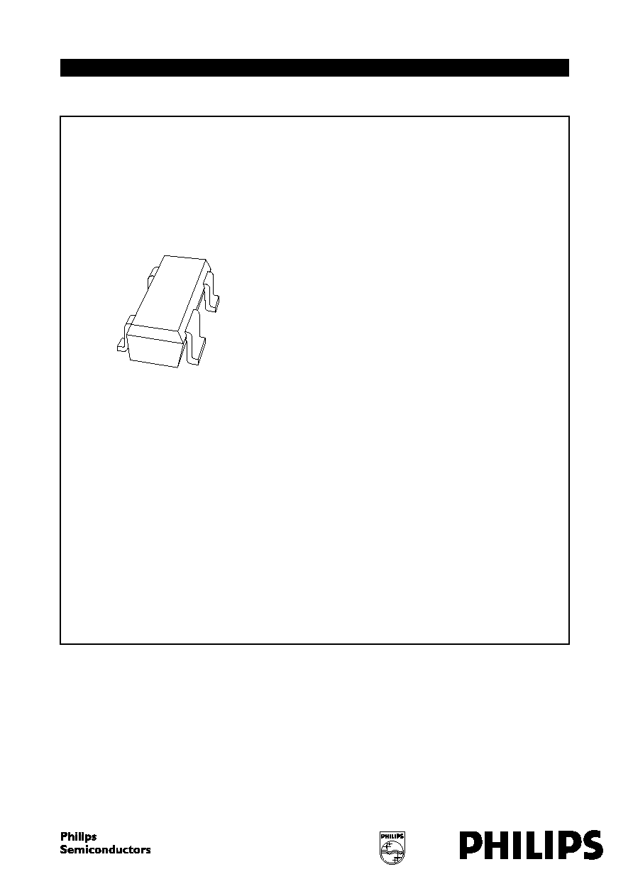
DESCRIPTION
NPN silicon planar epitaxial transistor
in a 4-pin dual-emitter SOT343N
plastic package.
PINNING
PIN
DESCRIPTION
BFG25AW
1
collector
2
base
3
emitter
4
emitter
BFG25AW/X
1
collector
2
emitter
3
base
4
emitter
MARKING
TYPE NUMBER
CODE
BFG25AW
N6
BFG25AW/X
V1
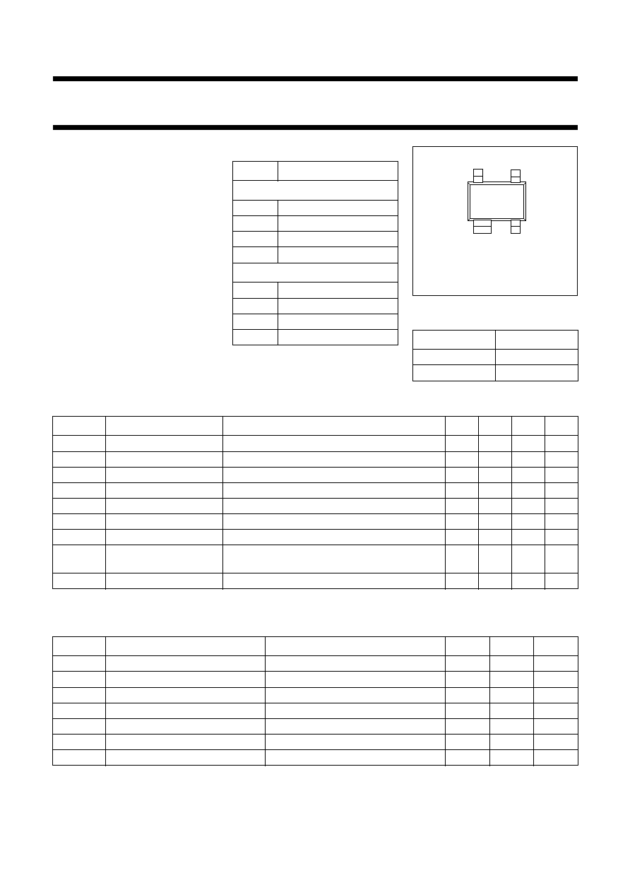
Fig.1 SOT343N.
fpage
Top view
MBK523
2
1
3
4
QUICK REFERENCE DATA
LIMITING VALUES
In accordance with the Absolute Maximum Rating System (IEC 134).
Note
1. T
s
is the temperature at the soldering point of the collector pin.
SYMBOL
PARAMETER
CONDITIONS
MIN.
TYP.
MAX. UNIT
V
CBO
collector-base voltage
open emitter
-
-
8
V
V
CEO
collector-emitter voltage
open base
-
-
5
V
I
C
collector current (DC)
-
-
6.5
mA
P
tot
total power dissipation
T
s
85
∞
C
-
-
500
mW
h
FE
DC current gain
I
C
= 0.5 mA; V
CE
= 1 V
50
80
200
C
re
feedback capacitance
I
C
= 0; V
CE
= 1 V; f = 1 MHz
-
0.2
0.3
pF
f
T
transition frequency
I
C
= 1 mA; V
CE
= 1 V; f = 500 MHz; T
amb
= 25
∞
C 3.5
5
-
GHz
G
UM
maximum unilateral
power gain
I
C
= 0.5 mA; V
CE
= 1 V; f = 1 GHz; T
amb
= 25
∞
C
-
16
-
dB
F
noise figure
s
=
opt
; I
C
= 1 mA; V
CE
= 1 V; f = 1 GHz
-
2
-
dB
SYMBOL
PARAMETER
CONDITIONS
MIN.
MAX.
UNIT
V
CBO
collector-base voltage
open emitter
-
8
V
V
CEO
collector-emitter voltage
open base
-
5
V
V
EBO
emitter-base voltage
open collector
-
2
V
I
C
collector current (DC)
-
6.5
mA
P
tot
total power dissipation
T
s
85
∞
C; see Fig.2; note 1
-
500
mW
T
stg
storage temperature
-
65
+150
∞
C
T
j
junction temperature
-
175
∞
C
1998 Sep 23
3
Philips Semiconductors
Product specification
NPN 5 GHz wideband transistors
BFG25AW; BFG25AW/X
THERMAL CHARACTERISTICS
Note
1. T
s
is the temperature at the soldering point of the collector pin.
CHARACTERISTICS
T
j
= 25
∞
C unless otherwise specified.
Note
1. G
UM
is the maximum unilateral power gain, assuming S
12
is zero.
SYMBOL
PARAMETER
CONDITIONS
VALUE
UNIT
R
th j-s
thermal resistance from junction to soldering point T
s
85
∞
C; note 1
180
K/W
SYMBOL
PARAMETER
CONDITIONS
MIN.
TYP.
MAX.
UNIT
V
(BR)CBO
collector-base breakdown voltage
I
C
= 100
µ
A; I
E
= 0
-
-
8
V
V
(BR)CEO
collector-emitter breakdown voltage I
C
= 1 mA; I
B
= 0
-
-
5
V
V
(BR)EBO
emitter-base breakdown voltage
I
E
= 100
µ
A; I
C
= 0
-
-
2
V
I
CBO
collector leakage current
open emitter; V
CB
= 5 V; I
E
= 0
-
-
50
nA
h
FE
DC current gain
I
C
= 0.5 mA; V
CE
= 1 V
50
80
200
C
re
feedback capacitance
I
C
= 0; V
CE
= 1 V; f = 1 MHz
-
0.2
0.3
pF
f
T
transition frequency
I
C
= 1 mA; V
CE
= 1 V; f = 1 GHz;
T
amb
= 25
∞
C
3.5
5
-
GHz
G
UM
maximum unilateral power gain;
note 1
I
C
= 0.5 mA; V
CE
= 1 V;
f = 1 GHz; T
amb
= 25
∞
C
-
16
-
dB
I
C
= 0.5 mA; V
CE
= 1 V;
f = 2 GHz; T
amb
= 25
∞
C
-
8
-
dB
F
noise figure
s
=
opt
; I
C
= 0.5 mA; V
CE
= 1 V;
f = 1 GHz
-
1.9
-
dB
s
=
opt
; I
C
= 1 mA; V
CE
= 1 V;
f = 1 GHz
-
2
dB
G
UM
10
S
21
2
1
S
11
2
≠
(
)
1
S
22
2
≠
(
)
-------------------------------------------------------------- dB.
log
=
1998 Sep 23
4
Philips Semiconductors
Product specification
NPN 5 GHz wideband transistors
BFG25AW; BFG25AW/X
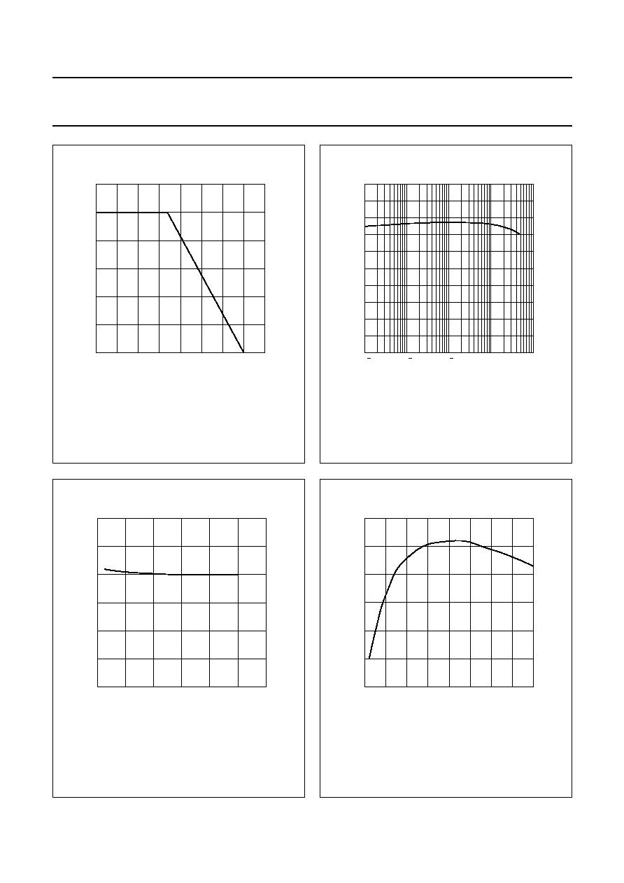
Fig.2 Power derating curve.
handbook, halfpage
0
50
100
200
400
0
MBG248
150
T ( C)
o
s
Ptot
(mW)
600
200
V
CE
= 1 V.
Fig.3
DC current gain as a function of collector
current; typical values.
handbook, halfpage
10
0
MCD138
1
10
1
10
2
10
3
40
100
h FE
I (mA)
C
20
80
60
I
C
= 0; f = 1 MHz.
Fig.4
Feedback capacitance as a function of
collector-base voltage; typical values.
handbook, halfpage
MLB971
0
2
4
6
0.3
0
0.2
V (V)
CE
Cre
(pF)
0.1
Fig.5
Transition frequency as a function of
collector current; typical values.
f = 500 MHz; V
CE
= 1 V; T
amb
= 25
∞
C.
handbook, halfpage
0
2
3
1
4
6
2
0
4
MLB972
(GHz)
T
f
I (mA)
C
1998 Sep 23
5
Philips Semiconductors
Product specification
NPN 5 GHz wideband transistors
BFG25AW; BFG25AW/X
f = 500 MHz; V
CE
= 1 V.
Fig.6
Gain as a function of collector current;
typical values.
handbook, halfpage
0
30
20
10
0
1
2
MLB973
3
gain
(dB)
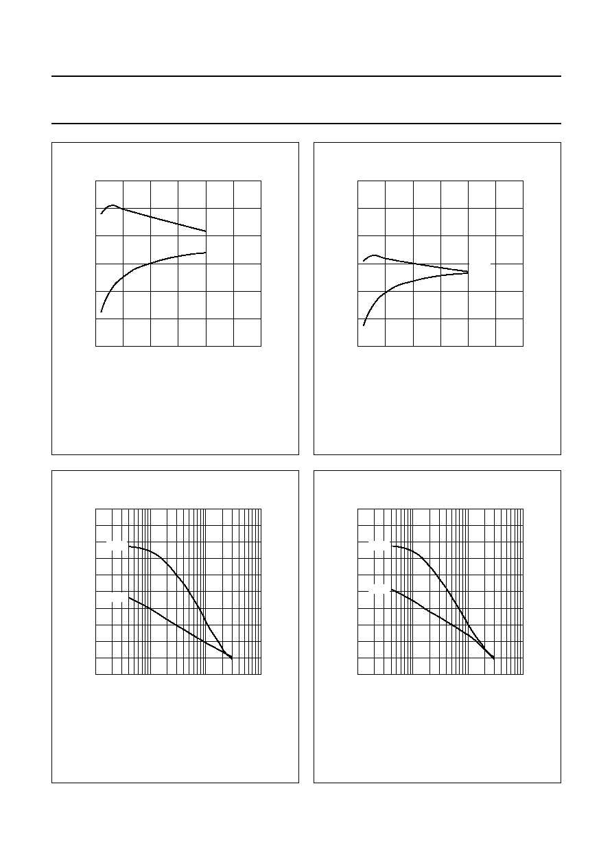
I (mA)
C
G UM
MSG
f = 1 GHz; V
CE
= 1 V.
Fig.7
Gain as a function of collector current;
typical values.
handbook, halfpage
0
30
20
10
0
1
2
MLB974
3
gain
(dB)
I (mA)
C
MSG
G UM
I
C
= 0.5 mA; V
CE
= 1 V.
Fig.8
Gain as a function of frequency;
typical values.
handbook, halfpage
50
0
10
MLB975
10
2
10
3
10
4
10
20
30
40
gain
(dB)
f (MHz)
G UM
MSG
Fig.9
Gain as a function of frequency;
typical values.
I
C
= 1 mA; V
CE
= 1 V.
handbook, halfpage
50
0
10
MLB976
10
2
10
3
10
4
10
20
30
40
gain
(dB)
f (MHz)
G UM
MSG