 | –≠–ª–µ–∫—Ç—Ä–æ–Ω–Ω—ã–π –∫–æ–º–ø–æ–Ω–µ–Ω—Ç: BFG31 | –°–∫–∞—á–∞—Ç—å:  PDF PDF  ZIP ZIP |

DATA SHEET
Product specification
Supersedes data of November 1992
File under Discrete Semiconductors, SC14
1995 Sep 12
DISCRETE SEMICONDUCTORS
BFG31
PNP 5 GHz wideband transistor

1995 Sep 12
2
Philips Semiconductors
Product specification
PNP 5 GHz wideband transistor
BFG31
FEATURES
∑
High output voltage capability
∑
High gain bandwidth product
∑
Good thermal stability
∑
Gold metallization ensures
excellent reliability.
DESCRIPTION
PNP planar epitaxial transistor
mounted in a plastic SOT223
envelope.
It is intended for wideband amplifier
applications.
NPN complement is the BFG97.
PINNING
PIN
DESCRIPTION
1
emitter
2
base
3
emitter
4
collector
Fig.1 SOT223.
page
4
1
2
3
MSB002 - 1
Top view
QUICK REFERENCE DATA
LIMITING VALUES
In accordance with the Absolute Maximum System (IEC 134).
Note
1. T
s
is the temperature at the soldering point of the collector tab.
SYMBOL
PARAMETER
CONDITIONS
MIN.
TYP.
MAX.
UNIT
V
CEO
collector-emitter voltage
open base
-
-
-
15
V
I
C
DC collector current
-
-
-
100
mA
P
tot
total power dissipation
up to T
s
= 135
∞
C ; note 1
-
-
1
W
h
FE
DC current gain
I
C
=
-
70 mA; V
CE
=
-
10 V;
T
amb
= 25
∞
C
25
-
-
f
T
transition frequency
I
C
=
-
70 mA; V
CE
=
-
10 V;
f = 500 MHz; T
amb
= 25
∞
C
-
5.0
-
GHz
G
UM
maximum unilateral power
gain
I
C
=
-
70 mA; V
CE
=
-
10 V;
f = 800 MHz; T
amb
= 25
∞
C
-
12
-
dB
V
o
output voltage
I
C
=
-
100 mA; V
CE
=
-
10 V;
R
L
= 75
; T
amb
= 25
∞
C
-
600
-
mV
SYMBOL
PARAMETER
CONDITIONS
MIN.
MAX.
UNIT
V
CBO
collector-base voltage
open emitter
-
-
20
V
V
CEO
collector-emitter voltage
open base
-
-
15
V
V
EBO
emitter-base voltage
open collector
-
-
3
V
I
C
DC collector current
-
-
100
mA
P
tot
total power dissipation
up to T
s
= 135
∞
C; note 1
-
1
W
T
stg
storage temperature
-
65
150
∞
C
T
j
junction temperature
-
175
∞
C
1995 Sep 12
3
Philips Semiconductors
Product specification
PNP 5 GHz wideband transistor
BFG31
THERMAL CHARACTERISTICS
Note
1. T
s
is the temperature at the soldering point of the collector tab.
CHARACTERISTICS
T
j
= 25
∞
C unless otherwise specified.
Notes
1. G
UM
is the maximum unilateral power gain, assuming S
12
is zero and
2. d
im
=
-
60 dB; I
C
=
-
70 mA; V
CE
=
-
10 V; R
L
= 75
; T
amb
= 25
∞
C;
V
p
= V
o
at d
im
=
-
60 dB; f
p
= 850.25 MHz;
V
q
= V
o
-
6 dB; f
q
= 858.25 MHz;
V
r
= V
o
-
6 dB;f
r
= 860.25 MHz;
measured at f
(p+q
-
r)
= 848.25 MHz.
3. d
im
=
-
60 dB (DIN 45004B); I
C
=
-
70 mA; V
CE
=
-
10 V; R
L
= 75
; T
amb
= 25
∞
C;
V
p
= V
o
= at d
im
=
-
60 dB; f
p
= 445.25 MHz;
V
q
= V
o
-
6 dB; f
q
= 453.25 MHz;
V
r
= V
o
-
6 dB; f
r
= 455.25 MHz;
measured at f
(p+q
-
r)
= 443.25 MHz.
SYMBOL
PARAMETER
CONDITIONS
THERMAL RESISTANCE
R
th j-s
thermal resistance from junction to
soldering point
up to T
s
= 135
∞
C; note 1
40 K/W
SYMBOL
PARAMETER
CONDITIONS
MIN.
TYP.
MAX.
UNIT
V
(BR)CBO
collector-base breakdown voltage
open emitter; I
C
=
-
10 mA
-
20
-
-
V
V
(BR)CEO
collector-emitter breakdown voltage
open base; I
C
=
-
10 mA
-
18
-
-
V
V
(BR)EBO
emitter-base breakdown voltage
open collector; I
E
=
-
0.1 mA
-
3
-
-
V
I
CBO
collector cut-off current
I
E
= 0; V
CB
=
-
10 V
-
-
-
1
µ
A
h
FE
DC current gain
I
C
=
-
70 mA; V
CE
=
-
10 V;
T
amb
= 25
∞
C
25
-
-
C
cb
collector-base capacitance
I
C
= 0; V
CB
=
-
10 V; f = 1 MHz;
-
1.8
-
pF
C
eb
emitter-base capacitance
I
C
= 0; V
EB
=
-
10 V; f = 1 MHz
-
5
-
pF
C
re
feedback capacitance
I
C
= 0; V
CE
=
-
10 V; f = 1 MHz;
T
amb
= 25
∞
C
-
1.6
-
pF
f
T
transition frequency
I
C
=
-
70 mA; V
CE
=
-
10 V;
f = 500 MHz; T
amb
= 25
∞
C
-
5
-
GHz
G
UM
maximum unilateral power gain; note 1
I
C
=
-
70 mA; V
CE
=
-
10 V;
f = 500 MHz; T
amb
= 25
∞
C
-
16
-
dB
I
C
=
-
70 mA; V
CE
=
-
10 V;
f = 800 MHz; T
amb
= 25
∞
C
-
12
-
dB
V
o
output voltage
note 2
-
600
-
mV
V
o
output voltage
note 3
-
550
-
mV
G
UM
10
s
21
2
1
s
11
2
≠
(
)
1
s
22
2
≠
(
)
------------------------------------------------------------ dB.
log
=
1995 Sep 12
4
Philips Semiconductors
Product specification
PNP 5 GHz wideband transistor
BFG31
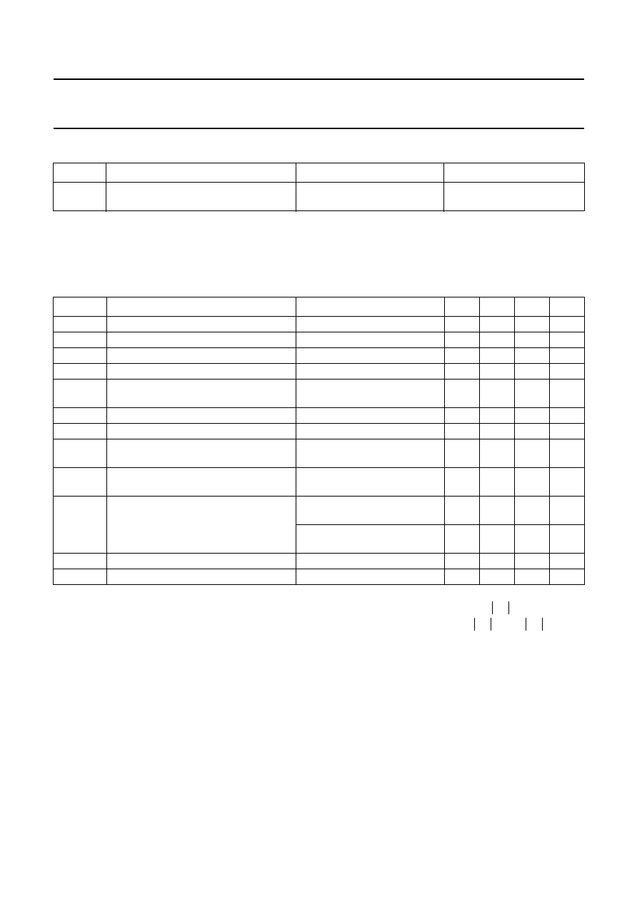
Fig.2 Power derating curve.
handbook, halfpage
0
50
100
200
0.8
0.6
0.2
0
0.4
MBB344
150
T ( C)
o
s
Ptot
(W)
1.0
1.2
Fig.3
DC current gain as a function of collector
current.
V
CE
=
-
10 V; T
amb
= 25
∞
C.
handbook, halfpage
MBB345
0
80
60
20
0
100
200
FE
h
40
I (mA)
C
Fig.4
Feedback capacitance as a function of
collector-emitter voltage.
f = 1 MHz; T
amb
= 25
∞
C
handbook, halfpage
0
6
1
30
MBB346
10
20
C re
(pF)
5
4
3
2
V (V)
CE
Fig.5
Transition frequency as a function of
collector current.
V
CE
=
-
10 V; T
amb
= 25
∞
C.
handbook, halfpage
0
50
100
8
6
2
0
4
MBB347
(GHz)
T
f
I (mA)
C
1995 Sep 12
5
Philips Semiconductors
Product specification
PNP 5 GHz wideband transistor
BFG31
Fig.6
Intermodulation distortion as a function
of collector current.
V
CE
=
-
10 V; V
o
= 650 mV; T
amb
= 25
∞
C;
f
(p+q
-
r)
= 443.25 MHz.
handbook, halfpage
MBB348
(dB)
40
60
100
40
65
45
80
50
55
60
d im
I (mA)
C
Fig.7
Intermodulation distortion as a function
of collector current.
V
CE
=
-
10 V; V
o
= 550 mV; T
amb
= 25
∞
C;
f
(p+q
-
r)
= 848.25 MHz.
handbook, halfpage
MBB349
(dB)
40
60
80
120
50
100
55
60
65
d im
I (mA)
C
Fig.8 Second order intermodulation distortion
as a function of collector current.
V
CE
=
-
10 V; V
o
= 50 dBmV; T
amb
= 25
∞
C;
f
(p+q)
= 450 MHz.
handbook, halfpage
MBB350
10
110
10
60
50
40
30
20
30
50
70
90
d 2
(dB)
I (mA)
C
Fig.9
Second order intermodulation distortion
as a function of collector current.
V
CE
=
-
10 V; V
o
= 50 dBmV; T
amb
= 25
∞
C;
f
(p+q)
= 810 MHz.
handbook, halfpage
MBB351
10
110
10
60
50
40
30
20
30
50
70
90
d 2
(dB)
I (mA)
C