BFG325W/XR
NPN 14 GHz wideband transistor
1.
Product profile
1.1 General description
NPN silicon planar epitaxial transistor in a 4-pin dual-emitter SOT343R plastic package.
1.2 Features
s
High power gain
s
Low noise figure
s
High transition frequency
s
Gold metallization ensures excellent reliability
1.3 Applications
s
Intended for Radio Frequency (RF) front end applications in the GHz range, such as:
x
analog and digital cellular telephones
x
cordless telephones (Cordless Telephone (CT), Personal Communication
Network (PCN), Digital Enhanced Cordless Telecommunications (DECT), etc.)
x
radar detectors
x
pagers
x
Satellite Antenna TeleVision (SATV) tuners
1.4 Quick reference data
BFG325W/XR
NPN 14 GHz wideband transistor
Rev. 01 -- 2 February 2005
Product data sheet
Table 1:
Quick reference data
Symbol Parameter
Conditions
Min
Typ
Max
Unit
V
CBO
collector-base voltage
open emitter
-
-
15
V
V
CEO
collector-emitter voltage
open base
-
-
6
V
I
C
collector current (DC)
-
-
35
mA
P
tot
total power dissipation
T
sp
90
°
C
[1]
-
-
210
mW
h
FE
DC current gain
I
C
= 15 mA; V
CE
= 3 V;
T
j
= 25
°
C
60
100
200
C
CBS
collector-base
capacitance
V
CB
= 5 V; f = 1 MHz;
emitter grounded
-
0.27
0.4
pF
f
T
transition frequency
I
C
= 15 mA; V
CE
= 3 V;
f = 1 GHz; T
amb
= 25
°
C
-
14
-
GHz
G
max
maximum power gain
[2]
I
C
= 15 mA; V
CE
= 3 V;
f = 1.8 GHz; T
amb
= 25
°
C
-
18.3
-
dB
9397 750 14246
© Koninklijke Philips Electronics N.V. 2005. All rights reserved.
Product data sheet
Rev. 01 -- 2 February 2005
2 of 12
Philips Semiconductors
BFG325W/XR
NPN 14 GHz wideband transistor
[1]
T
sp
is the temperature at the soldering point of the collector pin.
[2]
G
max
is the maximum power gain, if K > 1. If K < 1 then G
max
= MSG, see
Figure 4
.
2.
Pinning information
3.
Ordering information
4.
Marking
[1]
* = p: made in Hong Kong.
5.
Limiting values
|
s
21
|
2
insertion power gain
I
C
= 15 mA; V
CE
= 3 V;
f = 1.8 GHz; T
amb
= 25
°
C;
Z
S
= Z
L
= 50
-
14
-
dB
NF
noise figure
s
=
opt
; I
C
= 3 mA;
V
CE
= 3 V; f = 2 GHz
-
1.1
-
dB
Table 1:
Quick reference data
...continued
Symbol Parameter
Conditions
Min
Typ
Max
Unit
Table 2:
Pinning
Pin
Description
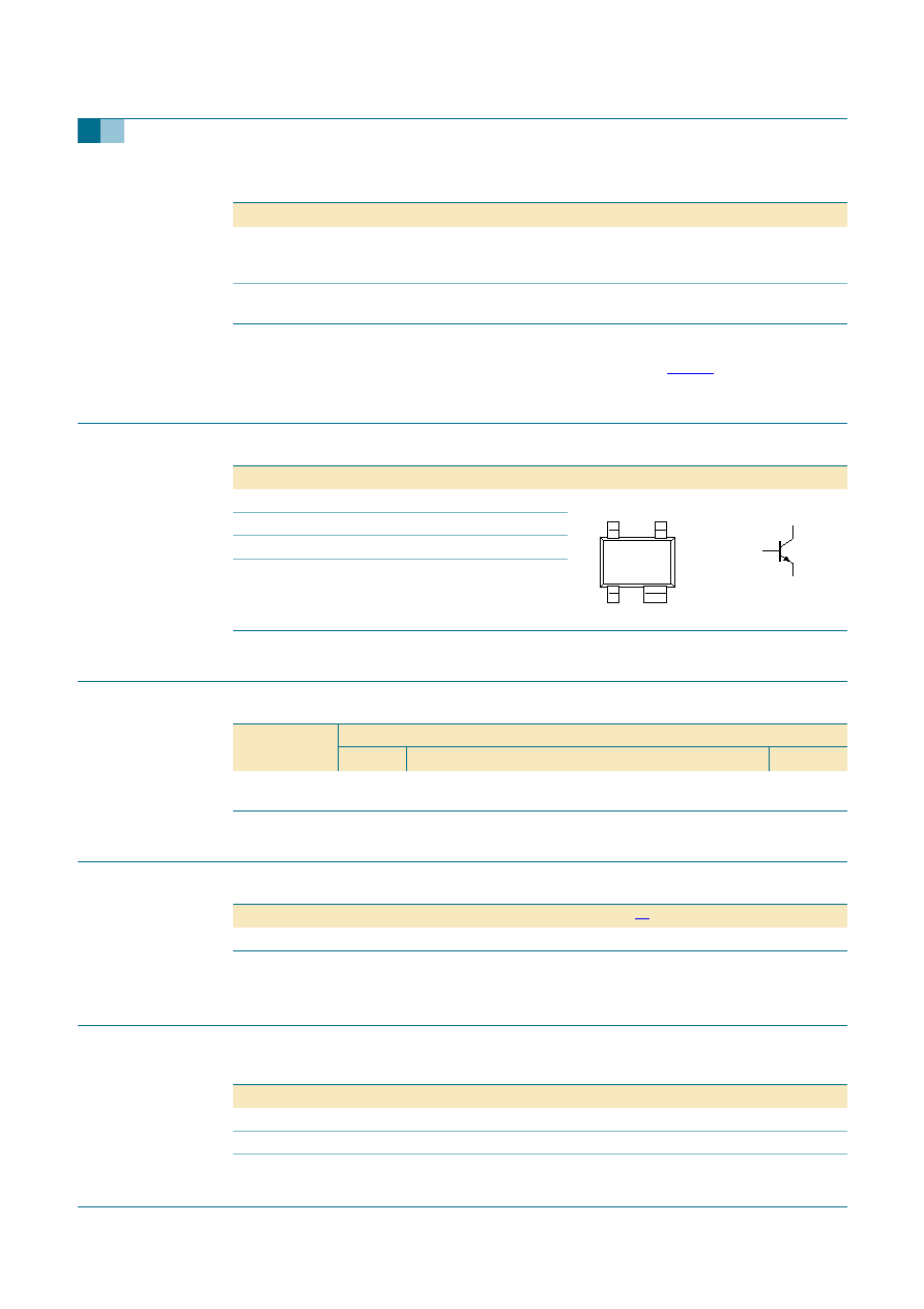
Simplified outline
Symbol
1
collector
2
emitter
3
base
4
emitter
2
1
4
3
sym086
1
2, 4
3
Table 3:
Ordering information
Type number
Package
Name
Description
Version
BFG325W/XR
-
plastic surface mounted package; reverse pinning;
4 leads
SOT343R
Table 4:
Marking codes
Type number
Marking code
[1]
BFG325W/XR
A8*
Table 5:
Limiting values
In accordance with the Absolute Maximum Rating System (IEC 60134).
Symbol
Parameter
Conditions
Min
Max
Unit
V
CBO
collector-base voltage
open emitter
-
15
V
V
CEO
collector-emitter voltage
open base
-
6
V
V
EBO
emitter-base voltage
open collector
-
2
V

9397 750 14246
© Koninklijke Philips Electronics N.V. 2005. All rights reserved.
Product data sheet
Rev. 01 -- 2 February 2005
3 of 12
Philips Semiconductors
BFG325W/XR
NPN 14 GHz wideband transistor
[1]
T
sp
is the temperature at the soldering point of the collector pin.
6.
Thermal characteristics
[1]
T
sp
is the temperature at the soldering point of the collector pin.
7.
Characteristics
[1]
G
max
is the maximum power gain, if K > 1. If K < 1 then G
max
= MSG, see
Figure 4
.
K is the Rollet stability factor:
where
.
MSG = maximum stable gain.
I
C
collector current (DC)
-
35
mA
P
tot
total power dissipation
T
sp
90
°
C
[1]
-
210
mW
T
stg
storage temperature
-
65
+175
°
C
T
j
junction temperature
-
175
°
C
Table 5:
Limiting values
...continued
In accordance with the Absolute Maximum Rating System (IEC 60134).
Symbol
Parameter
Conditions
Min
Max
Unit
Table 6:
Thermal characteristics
Symbol Parameter
Conditions
Typ
Unit
R
th(j-sp)
thermal resistance from junction to solder point
T
sp
90
°
C
[1]
403
K/W
Table 7:
Characteristics
T
j
= 25
°
C; unless otherwise specified.
Symbol Parameter
Conditions
Min
Typ
Max
Unit
I
CBO
collector-base cut-off current
I
E
= 0 A; V
CB
= 5 V
-
-
15
nA
h
FE
DC current gain
I
C
= 15 mA; V
CE
= 3 V
60
100
200
C
CBS
collector-base capacitance
V
CB
= 5 V; f = 1 MHz; emitter grounded
-
0.27
0.4
pF
C
CES
collector-emitter capacitance
V
CE
= 5 V; f = 1 MHz; base grounded
-
0.22
-
pF
C
EBS
emitter-base capacitance
V
EB
= 0.5 V; f = 1 MHz; collector grounded
-
0.49
-
pF
f
T
transition frequency
I
C
= 15 mA; V
CE
= 3 V; f = 1 GHz;
T
amb
= 25
°
C
-
14
-
GHz
G
max
maximum power gain
[1]
I
C
= 15 mA; V
CE
= 3 V; f = 1.8 GHz;
T
amb
= 25
°
C
-
18.3
-
dB
|
s
21
|
2
insertion power gain
I
C
= 15 mA; V
CE
= 3 V; T
amb
= 25
°
C;
Z
S
= Z
L
= 50
f = 1.8 GHz
-
14
-
dB
f = 3 GHz
-
10
-
dB
NF
noise figure
s
=
opt
; I
C
= 3 mA; V
CE
= 3 V; f = 2 GHz
-
1.1
-
dB
P
L(1dB)
output power at 1 dB gain
compression
I
C
= 15 mA; V
CE
= 3 V; f = 1.8 GHz;
T
amb
= 25
°
C; Z
S
= Z
L
= 50
-
8.7
-
dBm
IP3
third order intercept point
I
C
= 15 mA; V
CE
= 3 V; f = 1.8 GHz;
T
amb
= 25
°
C; Z
S
= Z
L
= 50
-
19.4
-
dBm
K
1
Ds
2
s
11
2
s
22
2
+
2
s
21
×
s
12
×
-----------------------------------------------------------
=
Ds
s
11
s
22
×
s
12
s
21
×
=
9397 750 14246
© Koninklijke Philips Electronics N.V. 2005. All rights reserved.
Product data sheet
Rev. 01 -- 2 February 2005
4 of 12
Philips Semiconductors
BFG325W/XR
NPN 14 GHz wideband transistor
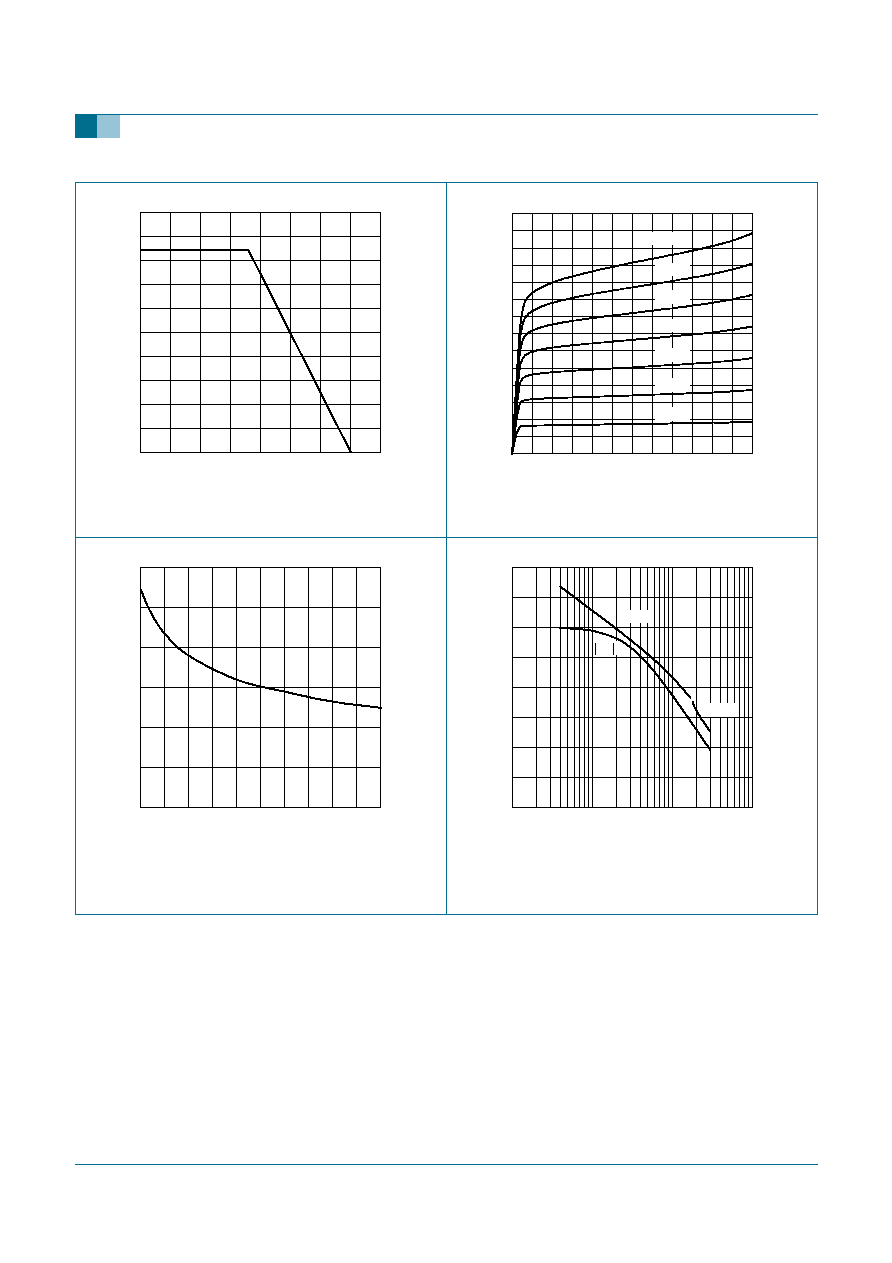
Fig 1.
Power derating curve
Fig 2.
Collector current as a function of
collector-emitter voltage; typical values
I
C
= 0 mA; f = 1 MHz.
I
C
= 15 mA; V
CE
= 3 V.
Fig 3.
Collector-base capacitance as a function of
collector-base voltage; typical values
Fig 4.
Gain as a function of frequency; typical values
T
sp
(
°
C)
0
200
150
50
100
001aac158
100
150
50
200
250
P
tot
(mW)
0
001aac159
V
CE
(V)
0
6
5
3
1
4
2
I
C
(mA)
10
15
20
25
5
30
35
0
I
B
= 350
µ
A
300
µ
A
250
µ
A
150
µ
A
100
µ
A
200
µ
A
50
µ
A
V
CB
(V)
0
5
4
2
3
1
001aac160
0.26
0.30
0.34
C
CBS
(pF)
0.22
001aac161
20
10
30
40
G
(dB)
0
f (MHz)
10
10
4
10
3
10
2
G
max
MSG
s
21
2
9397 750 14246
© Koninklijke Philips Electronics N.V. 2005. All rights reserved.
Product data sheet
Rev. 01 -- 2 February 2005
5 of 12
Philips Semiconductors
BFG325W/XR
NPN 14 GHz wideband transistor
V
CE
= 3 V; I
C
= 15 mA; Z
o
= 50
.
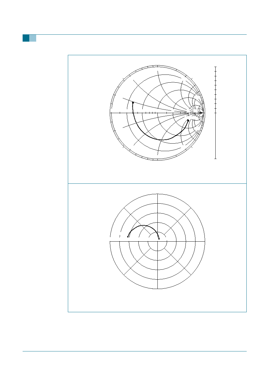
Fig 5.
Common emitter input reflection coefficient (s
11
); typical values
V
CE
= 3 V; I
C
= 15 mA.
Fig 6.
Common emitter forward transmission coefficient (s
21
); typical values
001aac162
90
°
-
90
°
5
0.5
0.2
+
0.2
0
+
2
+
5
-
5
-
2
-
0.2
+
0.5
-
0.5
+
1
-
1
2
1
10
0
0.2
0.6
0.4
0.8
1.0
1.0
-
45
°
-
135
°
45
°
135
°
180
°
0
°
3 GHz
40 MHz
001aac163
90
°
-
90
°
-
45
°
-
135
°
45
°
135
°
0
°
0
180
°
50
40
30
20
10
40 MHz
3 GHz
Document Outline