 | ÐлекÑÑоннÑй компоненÑ: BFG424W | СкаÑаÑÑ:  PDF PDF  ZIP ZIP |
Äîêóìåíòàöèÿ è îïèñàíèÿ www.docs.chipfind.ru
1.
Product profile
1.1 General description
NPN double polysilicon wideband transistor with buried layer for low voltage applications
in a plastic, 4-pin dual-emitter SOT343R package.
1.2 Features
s
Very high power gain
s
Low noise figure
s
High transition frequency
s
Emitter is thermal lead
s
Low feedback capacitance
1.3 Applications
s
Radio Frequency (RF) front end wideband applications such as:
x
analog and digital cellular telephones
x
cordless telephones (Cordless Telephone (CT), Personal Handy-phone
System (PHS), Digital Enhanced Cordless Telecommunications (DECT), etc.)
x
radar detectors
x
pagers
x
Satellite Antenna TeleVison (SATV) tuners
x
high frequency oscillators e.g. Dielectric Resonator Oscillator (DRO) for Low Noise
Block (LNB)
1.4 Quick reference data
BFG424W
NPN 25 GHz wideband transistor
Rev. 01 -- 21 March 2006
Product data sheet
CAUTION
This device is sensitive to ElectroStatic Discharge (ESD). Therefore care should be taken
during transport and handling.
MSC895
Table 1:
Quick reference data
Symbol
Parameter
Conditions
Min
Typ
Max
Unit
V
CBO
collector-base voltage
open emitter
-
-
10
V
V
CEO
collector-emitter voltage
open base
-
-
4.5
V
I
C
collector current
-
25
30
mA
P
tot
total power dissipation
T
sp
103
°
C
[1]
-
-
135
mW

BFG424W_1
© Koninklijke Philips Electronics N.V. 2006. All rights reserved.
Product data sheet
Rev. 01 -- 21 March 2006
2 of 13
Philips Semiconductors
BFG424W
NPN 25 GHz wideband transistor
[1]
T
sp
is the temperature at the soldering point of the emitter pins.
[2]
G
p(max)
is the maximum power gain, if K > 1. If K < 1 then G
p(max)
= Maximum Stable Gain (MSG), see
Figure 8
.
2.
Pinning information
3.
Ordering information
4.
Marking
[1]
* = p: made in Hong Kong.
h
FE
DC current gain
I
C
= 25 mA; V
CE
= 2 V;
T
j
= 25
°
C
50
80
120
C
CBS
collector-base
capacitance
V
CB
= 2 V; f = 1 MHz
-
105
-
fF
f
T
transition frequency
I
C
= 25 mA; V
CE
= 2 V;
f = 2 GHz; T
amb
= 25
°
C
-
25
-
GHz
G
p(max)
maximum power gain
I
C
= 25 mA; V
CE
= 2 V;
f = 2 GHz; T
amb
= 25
°
C
[2]
-
22
-
dB
NF
noise figure
I
C
= 2 mA; V
CE
= 2 V;
f = 2 GHz;
S
=
opt
-
1.2
-
dB
Table 1:
Quick reference data
...continued
Symbol
Parameter
Conditions
Min
Typ
Max
Unit
Table 2:
Pinning
Pin
Description
Simplified outline
Symbol
1
emitter
2
base
3
emitter
4
collector
2
1
4
3
mbb159
4
1, 3
2
Table 3:
Ordering information
Type number
Package
Name
Description
Version
BFG424W
-
plastic surface mounted package; reverse pinning;
4 leads
SOT343R
Table 4:
Marking
Type number
Marking code
[1]
BFG424W
ND*
BFG424W_1
© Koninklijke Philips Electronics N.V. 2006. All rights reserved.
Product data sheet
Rev. 01 -- 21 March 2006
3 of 13
Philips Semiconductors
BFG424W
NPN 25 GHz wideband transistor
5.
Limiting values
[1]
T
sp
is the temperature at the soldering point of the emitter pins.
6.
Thermal characteristics
[1]
T
sp
is the temperature at the soldering point of the emitter pins.
Table 5:
Limiting values
In accordance with the Absolute Maximum Rating System (IEC 60134).
Symbol
Parameter
Conditions
Min
Max
Unit
V
CBO
collector-base voltage
open emitter
-
10
V
V
CEO
collector-emitter voltage
open base
-
4.5
V
V
EBO
emitter-base voltage
open collector
-
1
V
I
C
collector current
-
30
mA
P
tot
total power dissipation
T
sp
103
°
C
[1]
-
135
mW
T
stg
storage temperature
-
65
+
150
°
C
T
j
junction temperature
-
150
°
C
Table 6:
Thermal characteristics
Symbol
Parameter
Conditions
Typ
Unit
R
th(j-sp)
thermal resistance from junction
to solder point
T
sp
103
°
C
[1]
340
K/W
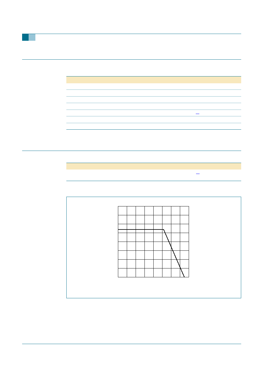
Fig 1.
Power derating curve
0
40
160
200
150
50
0
100
80
120
mgg681
T
sp
(
°
C)
P
tot
(mW)

BFG424W_1
© Koninklijke Philips Electronics N.V. 2006. All rights reserved.
Product data sheet
Rev. 01 -- 21 March 2006
4 of 13
Philips Semiconductors
BFG424W
NPN 25 GHz wideband transistor
7.
Characteristics
[1]
G
p(max)
is the maximum power gain, if K
>
1. If K
<
1 then G
p(max)
= MSG, see
Figure 8
.
[2]
Z
S
is optimized for noise; Z
L
is optimized for gain.
Table 7:
Characteristics
T
j
= 25
°
C; unless otherwise specified.
Symbol
Parameter
Conditions
Min
Typ
Max
Unit
V
(BR)CBO
collector-base
breakdown voltage
I
C
= 2.5
µ
A; I
E
= 0 mA
10
-
-
V
V
(BR)CEO
collector-emitter
breakdown voltage
I
C
= 1 mA; I
B
= 0 mA
4.5
-
-
V
V
(BR)EBO
open-collector
emitter-base
breakdown voltage
I
E
= 2.5
µ
A; I
C
= 0 mA
1
-
-
V
I
CBO
collector-base
cut-off current
I
E
= 0 mA; V
CB
= 4.5 V
-
-
15
nA
h
FE
DC current gain
I
C
= 25 mA; V
CE
= 2 V
50
80
120
C
CES
collector-emitter
capacitance
V
CB
= 2 V; f = 1 MHz
-
385
-
fF
C
EBS
emitter-base
capacitance
V
EB
= 0.5 V; f = 1 MHz
-
515
-
fF
C
CBS
collector-base
capacitance
V
CB
= 2 V; f = 1 MHz
-
105
-
fF
f
T
transition frequency I
C
= 25 mA; V
CE
= 2 V; f = 2 GHz;
T
amb
= 25
°
C
-
25
-
GHz
G
p(max)
maximum power
gain
I
C
= 25 mA; V
CE
= 2 V; f = 2 GHz;
T
amb
= 25
°
C
[1]
-
22
-
dB
|
s
21
|
2
insertion power gain I
C
= 25 mA; V
CE
= 2 V; f = 2 GHz;
T
amb
= 25
°
C
-
18
-
dB
NF
noise figure
I
C
= 2 mA; V
CE
= 2 V;
f = 900 MHz;
S
=
opt
-
0.8
-
dB
I
C
= 2 mA; V
CE
= 2 V; f = 2 GHz;
S
=
opt
-
1.2
-
dB
P
L(1dB)
output power at
1 dB gain
compression
I
C
= 25 mA; V
CE
= 2 V; f = 2 GHz;
Z
S
= Z
S(opt)
; Z
L
= Z
L(opt)
[2]
-
12
-
dBm
IP3
third-order intercept
point
I
C
= 25 mA; V
CE
= 2 V; f = 2 GHz;
Z
S
= Z
S(opt)
; Z
L
= Z
L(opt)
[2]
-
22
-
dBm
BFG424W_1
© Koninklijke Philips Electronics N.V. 2006. All rights reserved.
Product data sheet
Rev. 01 -- 21 March 2006
5 of 13
Philips Semiconductors
BFG424W
NPN 25 GHz wideband transistor
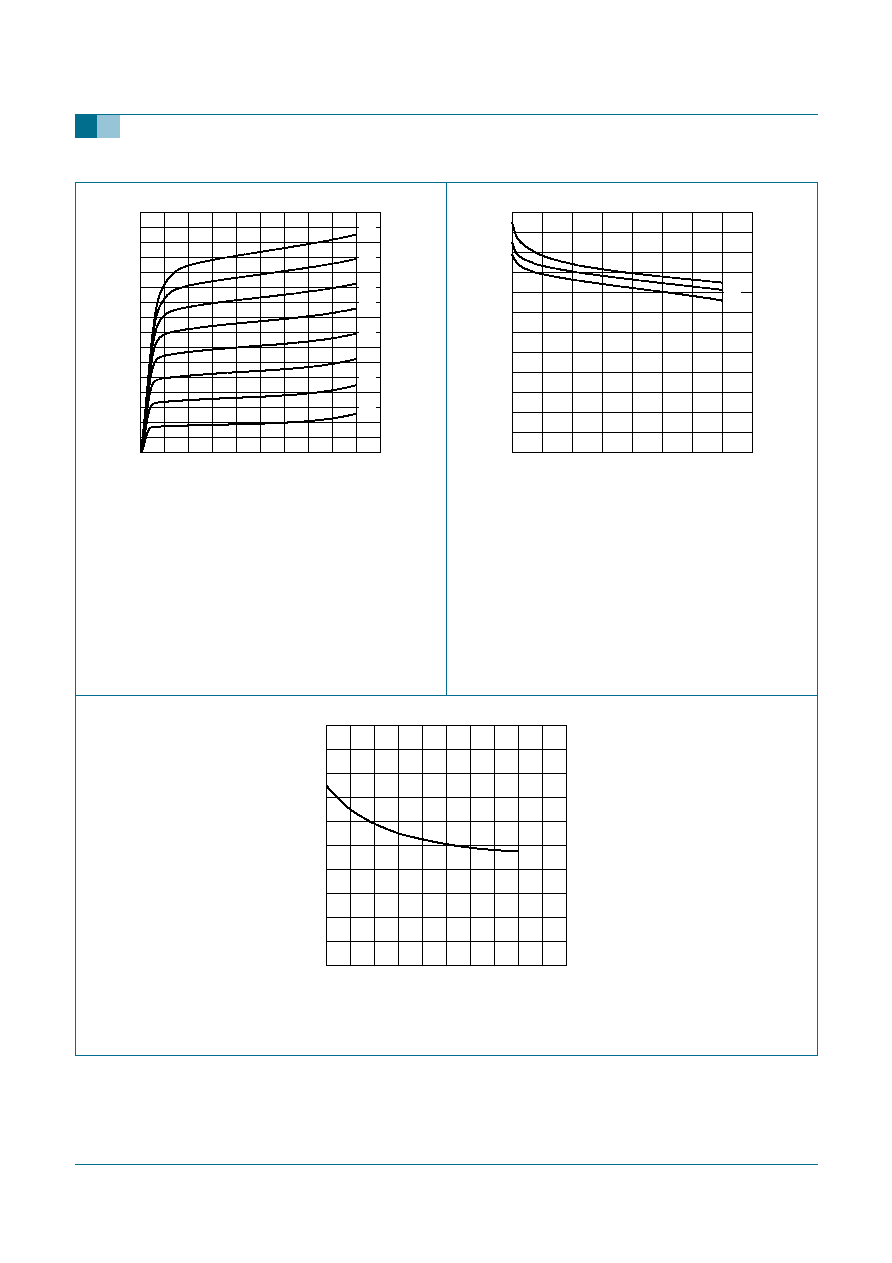
(1) I
B
= 400
µ
A
(2) I
B
= 350
µ
A
(3) I
B
= 300
µ
A
(4) I
B
= 250
µ
A
(5) I
B
= 200
µ
A
(6) I
B
= 150
µ
A
(7) I
B
= 100
µ
A
(8) I
B
= 50
µ
A
(1) V
CE
= 3 V
(2) V
CE
= 2 V
(3) V
CE
= 1 V
Fig 2.
Collector current as a function of
collector-emitter voltage; typical values
Fig 3.
DC current gain as a function of collector
current; typical values
f = 1 MHz
Fig 4.
Collector-base capacitance as a function of collector-base voltage; typical values
V
CE
(V)
0
5
4
2
3
1
001aad805
20
10
30
40
I
C
(mA)
0
(1)
(2)
(3)
(4)
(5)
(6)
(7)
(8)
I
C
(mA)
0
40
30
10
20
001aad806
40
80
120
h
FE
0
(1)
(2)
(3)
V
CB
(V)
0
5
4
2
3
1
001aad807
80
120
40
160
200
C
CBS
(fF)
0
Document Outline