 | –≠–ª–µ–∫—Ç—Ä–æ–Ω–Ω—ã–π –∫–æ–º–ø–æ–Ω–µ–Ω—Ç: BFG520W | –°–∫–∞—á–∞—Ç—å:  PDF PDF  ZIP ZIP |

DATA SHEET
Product specification
Supersedes data of August 1995
1998 Oct 02
DISCRETE SEMICONDUCTORS
BFG520W; BFG520W/X
NPN 9 GHz wideband transistors
book, halfpage
M3D123
1998 Oct 02
2
Philips Semiconductors
Product specification
NPN 9 GHz wideband transistors
BFG520W; BFG520W/X
FEATURES
∑
High power gain
∑
Low noise figure
∑
High transition frequency
∑
Gold metallization ensures excellent reliability.
APPLICATIONS
RF front end wideband applications in the GHz range,
such as analog and digital cellular telephones, cordless
telephones (CT2, CT3, PCN, DECT, etc.), radar detectors,
pagers, satellite television tuners (SATV) and repeater
amplifiers in fibre-optic systems.
DESCRIPTION
NPN silicon planar epitaxial transistor in a 4-pin
dual-emitter SOT343N plastic package.
MARKING
TYPE NUMBER
CODE
BFG520W
N3
BFG520W/X
N4
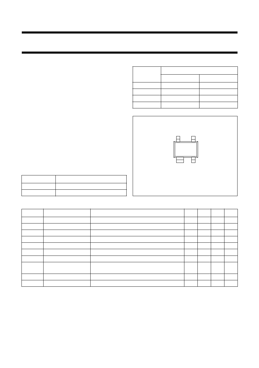
PINNING
PIN
DESCRIPTION
BFG250W
BFG250W/X
1
collector
collector
2
base
emitter
3
emitter
base
4
emitter
emitter
Fig.1 Simplified outline SOT343N.
handbook, halfpage
Top view
MBK523
2
1
3
4
QUICK REFERENCE DATA
SYMBOL
PARAMETER
CONDITIONS
MIN.
TYP.
MAX. UNIT
V
CBO
collector-base voltage
open emitter
-
-
20
V
V
CES
collector-emitter voltage R
BE
= 0
-
-
15
V
I
C
collector current (DC)
-
-
70
mA
P
tot
total power dissipation
T
s
85
∞
C
-
-
500
mW
h
FE
DC current gain
I
C
= 20 mA; V
CE
= 6 V
60
120
250
C
re
feedback capacitance
I
C
= 0; V
CB
= 6 V; f = 1 MHz
-
0.35
-
pF
f
T
transition frequency
I
C
= 20 mA; V
CE
= 6 V; f = 1 GHz; T
amb
= 25
∞
C
-
9
-
GHz
G
UM
maximum unilateral
power gain
I
C
= 20 mA; V
CE
= 6 V; f = 900 MHz; T
amb
= 25
∞
C
-
17
-
dB
|S
21
|
2
insertion power gain
I
C
= 20 mA; V
CE
= 6 V; f = 900 MHz; T
amb
= 25
∞
C 16
17
-
dB
F
noise figure
s
=
opt
; I
C
= 5 mA; V
CE
= 6 V; f = 900 MHz
-
1.1
1.6
dB
1998 Oct 02
3
Philips Semiconductors
Product specification
NPN 9 GHz wideband transistors
BFG520W; BFG520W/X
LIMITING VALUES
In accordance with the Absolute Maximum Rating System (IEC 134).
Note
1. T
s
is the temperature at the soldering point of the collector pin.
THERMAL CHARACTERISTICS
Note
1. T
s
is the temperature at the soldering point of the collector pin.
SYMBOL
PARAMETER
CONDITIONS
MIN.
MAX.
UNIT
V
CBO
collector-base voltage
open emitter
-
20
V
V
CES
collector-emitter voltage
R
BE
= 0
-
15
V
V
EBO
emitter-base voltage
open collector
-
2.5
V
I
C
collector current (DC)
-
70
mA
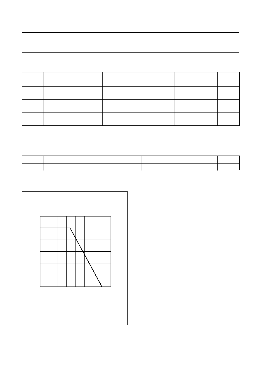
P
tot
total power dissipation
T
s
85
∞
C; see Fig.2; note 1
-
500
mW
T
stg
storage temperature
-
65
+150
∞
C
T
j
junction temperature
-
175
∞
C
SYMBOL
PARAMETER
CONDITIONS
VALUE
UNIT
R
th j-s
thermal resistance from junction to soldering point
T
s
85
∞
C; note 1
180
K/W
Fig.2 Power derating curve.
handbook, halfpage
0
50
100
200
400
0
MBG248
150
T ( C)
o
s
Ptot
(mW)
600
200

1998 Oct 02
4
Philips Semiconductors
Product specification
NPN 9 GHz wideband transistors
BFG520W; BFG520W/X
CHARACTERISTICS
T
j
= 25
∞
C unless otherwise specified.
Notes
1. G
UM
is the maximum unilateral power gain, assuming S
12
is zero.
2. I
C
= 20 mA; V
CE
= 6 V; R
L
= 50
; T
amb
= 25
∞
C;
f
p
= 900 MHz; f
q
= 902 MHz; measured at 2f
p
-
f
q
= 898 MHz and 2f
q
-
f
p
= 904 MHz.
3. d
im
=
-
60 dB (DIN45004B); I
C
= 20 mA; V
CE
= 6 V; V
p
= V
o
; V
q
= V
o
-
6 dB; V
r
= V
o
-
6 dB; R
L
= 75
;
f
p
= 795.25 MHz; f
q
= 803.25 MHz; f
r
= 805.25 MHz; measured at f
p
+ f
q
-
f
r
= 793.25 MHz.
4. I
C
= 20 mA; V
CE
= 6 V; V
o
= 75 mV; R
L
= 75
; T
amb
= 25
∞
C;
f
p
= 250 MHz; f
q
= 560 MHz; measured at f
p
+ f
q
= 810 MHz.
SYMBOL
PARAMETER
CONDITIONS
MIN.
TYP.
MAX.
UNIT
V
(BR)CBO
collector-base breakdown voltage
I
C
=10
µ
A; I
E
= 0
20
-
-
V
V
(BR)CES
collector-emitter breakdown voltage I
C
= 10
µ
A; R
BE
= 0
15
-
-
V
V
(BR)EBO
emitter-base breakdown voltage
I
E
= 10
µ
A; I
C
= 0
2.5
-
-
V
I
CBO
collector leakage current
V
CB
= 6 V; I
E
= 0
-
-
50
nA
h
FE
DC current gain
I
C
= 20 mA; V
CE
= 6 V; see Fig.3
60
120
250
C
re
feedback capacitance
I
C
= 0; V
CB
= 6 V; f = 1 MHz;
see Fig.4
-
0.35
-
pF
f
T
transition frequency
I
C
= 20 mA; V
CE
= 6 V; f = 1 GHz;
T
amb
= 25
∞
C; see Fig.5
-
9
-
GHz
G
UM
maximum unilateral power gain;
note 1
I
C
= 20 mA; V
CE
= 6 V; f = 900 MHz;
T
amb
= 25
∞
C
-
17
-
dB
I
C
= 20 mA; V
CE
= 6 V; f = 2 GHz;
T
amb
= 25
∞
C
-
11
-
dB
|S
21
|
2
insertion power gain
I
C
= 20 mA; V
CE
= 6 V; f = 900 MHz;
T
amb
= 25
∞
C
16
17
-
dB
F
noise figure
s
=
opt
; I
C
= 5 mA; V
CE
= 6 V;
f = 900 MHz
-
1.1
1.6
dB
s
=
opt
; I
C
= 20 mA; V
CE
= 6 V;
f = 900 MHz
-
1.6
2.1
dB
s
=
opt
; I
C
= 5 mA; V
CE
= 6 V;
f = 2 GHz
-
1.85
-
dB
P
L1
output power at 1 dB gain
compression
I
C
= 20 mA; V
CE
= 6 V; f = 900 MHz;
R
L
= 50
; T
amb
= 25
∞
C
-
17
-
dBm
ITO
third order intercept point
note 2
-
26
-
dBm
V
o
output voltage
note 3
-
275
-
mV
d
2
second order intermodulation
distortion
note 4
-
-
50
-
dB
G
UM
10
S
21
2
1
S
11
2
≠
(
)
1
S
22
2
≠
(
)
-------------------------------------------------------------- dB.
log
=
1998 Oct 02
5
Philips Semiconductors
Product specification
NPN 9 GHz wideband transistors
BFG520W; BFG520W/X
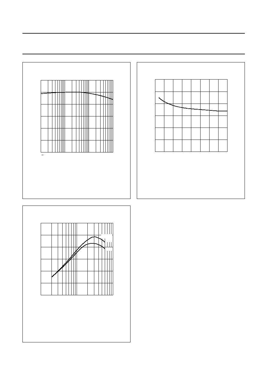
V
CE
= 6 V.
Fig.3
DC current gain as a function of collector
current; typical values.
handbook, halfpage
150
0
50
100
10
1
MLB807
1
10
10
2
I (mA)
C
FE
h
I
C
= 0; f = 1 MHz.
Fig.4
Feedback capacitance as a function of
collector-base voltage; typical values.
handbook, halfpage
MLB808
0
0.6
0.4
0.2
0
2.5
5
7.5
10
V (V)
CB
C re
(pF)
Fig.5
Transition frequency as a function of
collector current; typical values.
f = 1 GHz; T
amb
= 25
∞
C.
handbook, halfpage
8
4
0
MLB809
12
f
(GHz)
10
2
10
1
T
I (mA)
C
V =
CE
3 V
6 V