 | –≠–ª–µ–∫—Ç—Ä–æ–Ω–Ω—ã–π –∫–æ–º–ø–æ–Ω–µ–Ω—Ç: BFG590/XR | –°–∫–∞—á–∞—Ç—å:  PDF PDF  ZIP ZIP |
Document Outline
- FEATURES
- APPLICATIONS
- DESCRIPTION
- MARKING
- PINNING
- QUICK REFERENCE DATA
- LIMITING VALUES
- THERMAL CHARACTERISTICS
- CHARACTERISTICS
- PACKAGE OUTLINE
- DEFINITIONS
- LIFE SUPPORT APPLICATIONS

DATA SHEET
Product specification
Supersedes data of 1995 Sep 19
1998 Oct 02
DISCRETE SEMICONDUCTORS
BFG590; BFG590/X
NPN 5 GHz wideband transistors
book, halfpage
M3D071
1998 Oct 02
2
Philips Semiconductors
Product specification
NPN 5 GHz wideband transistors
BFG590; BFG590/X
FEATURES
∑
High power gain
∑
Low noise figure
∑
High transition frequency
∑
Gold metallization ensures excellent reliability.
APPLICATIONS
∑
MATV/CATV amplifiers and RF communications
subscriber equipment in the GHz range
∑
Ideally suitable for use in class-A, (A)B and C amplifiers
with either pulsed or continuous drive.
DESCRIPTION
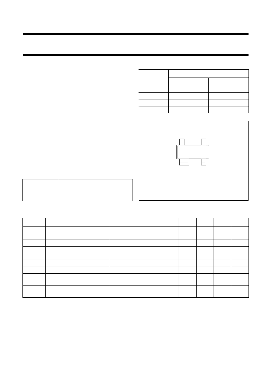
NPN silicon planar epitaxial transistor in a 4-pin
dual-emitter SOT143B plastic package.
MARKING
TYPE NUMBER
CODE
BFG590
N38
BFG590/X
N44
PINNING
PIN
DESCRIPTION
BFG590
BFG590/X
1
collector
collector
2
base
emitter
3
emitter
base
4
emitter
emitter
Fig.1 Simplified outline SOT143B.
handbook, 2 columns
Top view
MSB014
1
2
3
4
QUICK REFERENCE DATA
SYMBOL
PARAMETER
CONDITIONS
MIN.
TYP.
MAX.
UNIT
V
CBO
collector-base voltage
open emitter
-
-
20
V
V
CEO
collector-emitter voltage
open base
-
-
15
V
I
C
collector current (DC)
-
-
200
mA
P
tot
total power dissipation
T
s
60
∞
C
-
-
400
mW
h
FE
DC current gain
I
C
= 35 mA; V
CE
= 8 V
50
90
280
C
re
feedback capacitance
I
C
= 0; V
CE
= 8 V; f = 1 MHz
-
0.7
-
pF
f
T
transition frequency
I
C
= 80 mA; V
CE
= 4 V; f = 1 GHz
-
5
-
GHz
G
UM
maximum unilateral power gain
I
C
= 80 mA; V
CE
= 4 V;
f = 900 MHz; T
amb
= 25
∞
C
-
13
-
dB
|S
21
|
2
insertion power gain
I
C
= 80 mA; V
CE
= 4 V;
f = 900 MHz; T
amb
= 25
∞
C
-
11
-
dB
1998 Oct 02
3
Philips Semiconductors
Product specification
NPN 5 GHz wideband transistors
BFG590; BFG590/X
LIMITING VALUES
In accordance with the Absolute Maximum Rating System (IEC 134).
Note
1. T
s
is the temperature at the soldering point of the collector pin.
SYMBOL
PARAMETER
CONDITIONS
MIN.
MAX.
UNIT
V
CBO
collector-base voltage
open emitter
-
20
V
V
CEO
collector-emitter voltage
open base
-
15
V
V
EBO
emitter-base voltage
open collector
-
3
V
I
C
collector current (DC)
-
200
mA
P
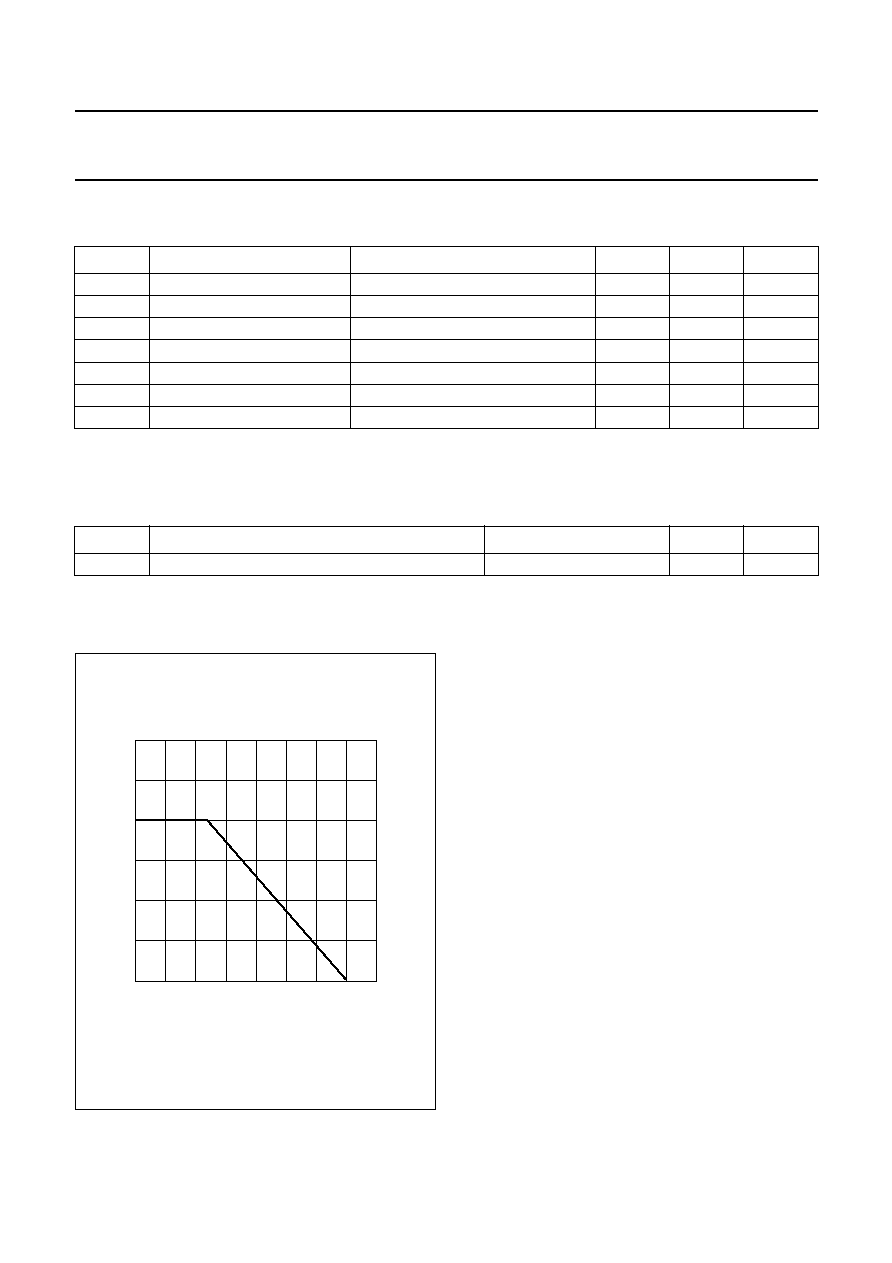
tot
total power dissipation
T
s
60
∞
C; see Fig.2; note 1
-
400
mW
T
stg
storage temperature
-
65
+150
∞
C
T
j
junction temperature
-
175
∞
C
Fig.2 Power derating curve.
handbook, halfpage
0
50
100
200
600
200
0
400
MBG249
150
P
tot
(mW)
T
s
(
o
C)
THERMAL CHARACTERISTICS
Note
1. T
s
is the temperature at the soldering point of the collector pin.
SYMBOL
PARAMETER
CONDITIONS
VALUE
UNIT
R
th j-s
thermal resistance from junction to soldering point
T
s
60
∞
C; note 1
290
K/W
1998 Oct 02
4
Philips Semiconductors
Product specification
NPN 5 GHz wideband transistors
BFG590; BFG590/X
CHARACTERISTICS
T
j
= 25
∞
C unless otherwise specified.
Note
1. G
UM
is the maximum unilateral power gain, assuming S
12
is zero and
SYMBOL
PARAMETER
CONDITIONS
MIN.
TYP.
MAX.
UNIT
V
(BR)CBO
collector-base breakdown voltage
I
C
= 0.1 mA; I
E
= 0
20
-
-
V
V
(BR)CEO
collector-emitter breakdown voltage I
C
= 10 mA; I
B
= 0
15
-
-
V
V
(BR)EBO
emitter-base breakdown voltage
I
E
= 0.1 mA; I
C
= 0
3
-
-
V
I
CBO
collector-base leakage current
V
CB
= 10 V; I
E
= 0
-
-
100
nA
h
FE
DC current gain
I
C
= 70 mA; V
CE
= 8 V; see Fig.3
60
120
250
f
T
transition frequency
I
C
= 80 mA; V
CE
= 4 V;
f = 1 GHz; see Fig.5
-
5
-
GHz
C
re
feedback capacitance
I
C
= 0; V
CB
= 8 V; f = 1 MHz;
see Fig.4
-
0.7
-
pF
G
UM
maximum unilateral power gain;
note 1
I
C
= 80 mA; V
CE
= 4 V;
f = 900 MHz; T
amb
= 25
∞
C
-
13
-
dB
I
C
= 80 mA; V
CE
= 4 V; f = 2 GHz;
T
amb
= 25
∞
C
-
7.5
-
dB
|S
21
|
2
insertion power gain
I
C
= 80 mA; V
CE
= 4 V;
f = 900 MHz; T
amb
= 25
∞
C
-
11
-
dB
G
UM
10
S
21
2
1
S
11
2
≠
(
)
1
S
22
2
≠
(
)
-------------------------------------------------------------- dB.
log
=
1998 Oct 02
5
Philips Semiconductors
Product specification
NPN 5 GHz wideband transistors
BFG590; BFG590/X
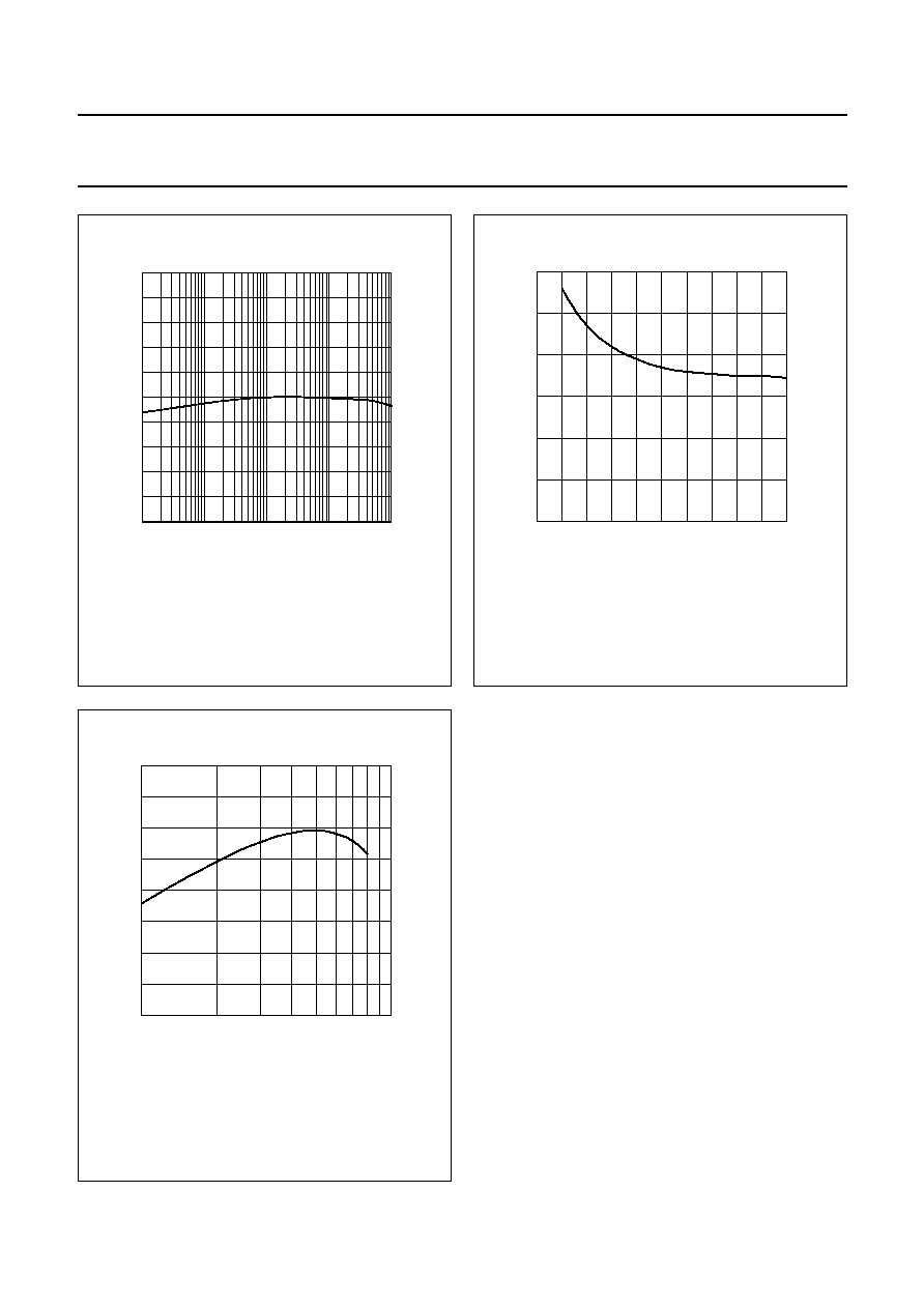
V
CE
= 8 V.
Fig.3
DC current gain as a function of collector
current; typical values.
handbook, halfpage
0
250
50
100
150
200
MRA749
10
-
2
10
-
1
1
10
10
2
hFE
IC (mA)
I
C
= 0; f = 1 MHz.
Fig.4
Feedback capacitance as a function of
collector-base voltage; typical values.
handbook, halfpage
0
1.2
0.8
0.4
0
2
10
MLC057
4
6
8
V (V)
CB
C re
(pF)
Fig.5
Transition frequency as a function of
collector current; typical values.
V
CE =
4 V; f = 1 GHz.
handbook, halfpage
8
0
4
6
10
MLC058
10
2
2
I (mA)
C
f
(GHz)
T