DATA SHEET
Product specification
File under Discrete Semiconductors, SC14
September 1995
DISCRETE SEMICONDUCTORS
BFG97
NPN 5 GHz wideband transistor
September 1995
2
Philips Semiconductors
Product specification
NPN 5 GHz wideband transistor
BFG97
DESCRIPTION
NPN planar epitaxial transistor
mounted in a plastic SOT223
envelope.
It features excellent output voltage
capabilities, and is primarily intended
for use in MATV applications.
PNP complement is the BFG31.
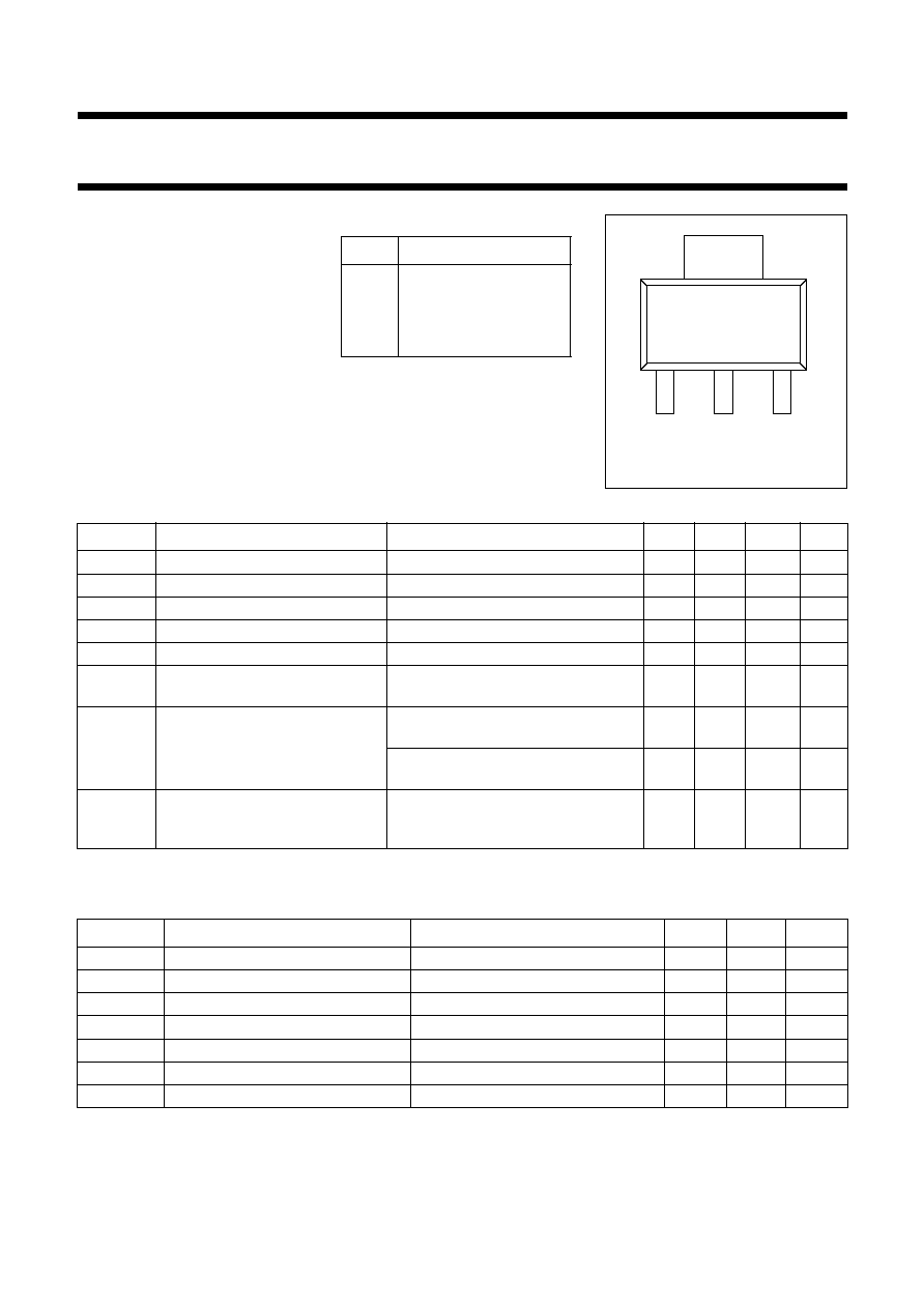
PINNING
PIN
DESCRIPTION
1
emitter
2
base
3
emitter
4
collector
Fig.1 SOT223.
age
4
1
2
3
MSB002 - 1
Top view
QUICK REFERENCE DATA
LIMITING VALUES
In accordance with the Absolute Maximum System (IEC 134).
Note
1. T
s
is the temperature at the soldering point of the collector tab.
SYMBOL
PARAMETER
CONDITIONS
MIN.
TYP.
MAX.
UNIT
V
CBO
collector-base voltage
open emitter
-
-
20
V
V
CEO
collector-emitter voltage
open base
-
-
15
V
I
C
DC collector current
-
-
100
mA
P
tot
total power dissipation
up to T
s
= 125
�
C (note 1)
-
-
1
W
h
FE
DC current gain
I
C
= 70 mA; V
CE
= 10 V; T
j
= 25
�
C
25
80
-
f
T
transition frequency
I
C
= 70 mA; V
CE
= 10 V;
f = 500 MHz; T
amb
= 25
�
C
-
5.5
-
GHz
G
UM
maximum unilateral power gain
I
C
= 70 mA; V
CE
= 10 V;
f = 500 MHz; T
amb
= 25
�
C
-
16
-
dB
I
C
= 70 mA; V
CE
= 10 V;
f = 800 MHz; T
amb
= 25
�
C
-
12
-
dB
V
o
output voltage
I
C
= 70 mA; V
CE
= 10 V;
d
im =
-
60 dB; R
L
= 75
;
f
(p
+
q
-
r)
= 793.25 MHz; T
amb
= 25
�
C
-
700
-
mV
SYMBOL
PARAMETER
CONDITIONS
MIN.
MAX.
UNIT
V
CBO
collector-base voltage
open emitter
-
20
V
V
CEO
collector-emitter voltage
open base
-
15
V
V
EBO
emitter-base voltage
open collector
-
3
V
I
C
DC collector current
-
100
mA
P
tot
total power dissipation
up to T
s
= 125
�
C (note 1)
-
1
W
T
stg
storage temperature
-
65
150
�
C
T
j
junction temperature
-
175
�
C

September 1995
3
Philips Semiconductors
Product specification
NPN 5 GHz wideband transistor
BFG97
THERMAL RESISTANCE
Note
1. T
s
is the temperature at the soldering point of the collector tab.
CHARACTERISTICS
T
j
= 25
�
C unless otherwise specified.
Notes
1. G
UM
is the maximum unilateral power gain, assuming S
12
is zero and
2. d
im
=
-
60 dB (DIN 45004B); I
C
= 70 mA; V
CE
= 10 V; R
L
= 75
; T
amb
= 25
�
C
V
p
= V
o
at d
im
=
-
60 dB;
V
q
= V
o
-
6 dB; f
p
= 445.25 MHz;
V
r
= V
o
-
6 dB; f
q
= 453.25 MHz; f
r
= 455.25 MHz;
measured at f
(p
+
q
-
r)
= 443.25 MHz.
3. d
im
=
-
60 dB (DIN 45004B); I
C
= 70 mA; V
CE
= 10 V; R
L
= 75
; T
amb
= 25
�
C
V
p
= V
o
at d
im
=
-
60 dB;
V
q
= V
o
-
6 dB; f
p
= 795.25 MHz;
V
r
= V
o
-
6 dB; f
q
= 803.25 MHz; f
r
= 805.25 MHz;
measured at f
(p
+
q
-
r)
= 793.25 MHz.
4. I
C
= 70 mA; V
CE
= 10 V; R
L
= 75
; T
amb
= 25
�
C;
V
p
= V
q
= V
o
= 50 dBmV; f
(p
+
q)
= 450 MHz; f
p
= 50 MHz; f
q
= 400 MHz.
5. I
C
= 70 mA; V
CE
= 10 V; R
L
= 75
; T
amb
= 25
�
C;
V
p
= V
q
= V
o
= 50 dBmV; f
(p
+
q)
= 810 MHz; f
p
= 250 MHz; f
q
= 560 MHz.
SYMBOL
PARAMETER
CONDITIONS
THERMAL RESISTANCE
R
th j-s
thermal resistance from junction to
soldering point
up to T
s
= 125
�
C (note 1)
50 K/W
SYMBOL
PARAMETER
CONDITIONS
MIN.
TYP.
MAX.
UNIT
I
CBO
collector cut-off current
I
E
= 0; V
CB
= 10 V
-
-
100
nA
h
FE
DC current gain
I
C
= 70 mA; V
CE
= 10 V
25
80
-
f
T
transition frequency
I
C
= 70 mA; V
CE
= 10 V;
f = 500 MHz; T
amb
= 25
�
C
-
5.5
-
GHz
C
c
collector capacitance
I
E
= i
e
= 0; V
CB
= 10 V; f = 1 MHz
-
1.5
-
pF
C
e
emitter capacitance
I
C
= i
c
= 0; V
EB
= 0.5 V; f = 1 MHz
-
6.5
-
pF
C
re
feedback capacitance
I
C
= 0; V
CE
= 10 V; f = 1 MHz
-
1
-
pF
G
UM
maximum unilateral power gain
(note 1)
I
C
= 70 mA; V
CE
= 10 V;
f = 500 MHz; T
amb
= 25
�
C
-
16
-
dB
I
C
= 70 mA; V
CE
= 10 V;
f = 800 MHz; T
amb
= 25
�
C
-
12
-
dB
V
o
output voltage
note 2
-
750
-
mV
note 3
-
700
-
mV
d
2
second order intermodulation
distortion
note 4
-
-
56
-
dB
note 5
-
-
53
-
dB
G
UM
10 log
S
21
2
1
S
11
2
�
1
S
22
2
�
--------------------------------------------------------------
dB.
=
September 1995
4
Philips Semiconductors
Product specification
NPN 5 GHz wideband transistor
BFG97
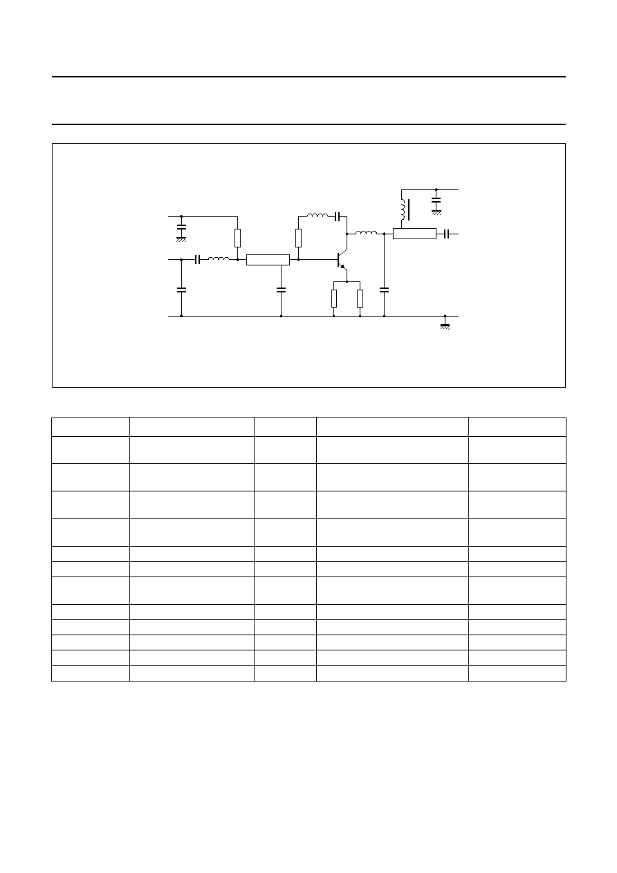
List of components (see test circuit)
Notes
The circuit has been built on a double copper-clad printed circuit board with PTFE dielectric (
r
= 2.2); thickness
1
/
16
inch;
thickness of copper sheet 2
�
35
�
m.
1. Components C5, L1, L4, L5, and R2 are mounted on the underside of the PCB.
DESIGNATION
DESCRIPTION
VALUE
DIMENSIONS
CATALOGUE NO.
C2, C3, C7, C8
multilayer ceramic
capacitor
10 nF
2222 590 08627
C1, C4, C6
multilayer ceramic
capacitor
1.2 pF
2222 851 12128
C5 (note 1)
miniature ceramic plate
capacitor
10 nF
2222 629 08103
L1 (note 1)
0.5 turns 0.4 mm copper
wire
int. dia. 3 mm
L2
microstripline
75
length 14 mm; width 2.5 mm
L3
microstripline
75
length 8 mm; width 2.5 mm
L4, L5 (note 1)
1.5 turns 0.4 mm copper
wire
int. dia. 3 mm;
winding pitch 1 mm
L6
microstripline
75
length 19 mm; width 2.5 mm
L7
Ferroxcube choke
5
�
H
3122 108 20153
R1
metal film resistor
10 k
2322 180 73103
R2 (note 1)
metal film resistor
220
2322 180 73221
R3, R4
metal film resistor
30
2322 180 73309
Fig.2 Intermodulation distortion and second order intermodulation distortion test circuit.
handbook, full pagewidth
MBB807
L1
C1
output
75
DUT
input
75
VCC
VBB
,
L4
C7
C8
L6
L5
C4
L2
R2
C5
R3
R4
C6
R1
L3
C3
C2
September 1995
5
Philips Semiconductors
Product specification
NPN 5 GHz wideband transistor
BFG97
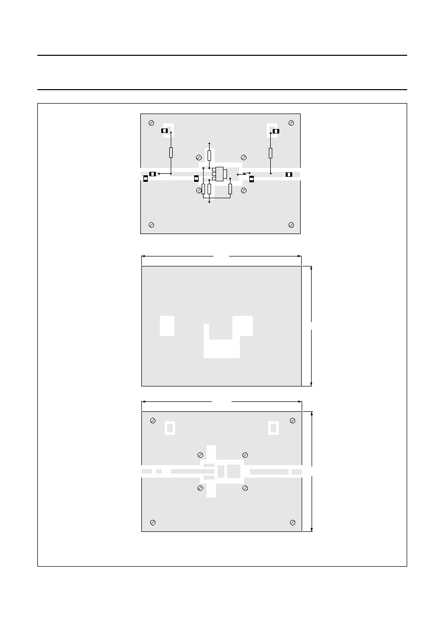
Fig.3 Intermodulation distortion and second order intermodulation distortion printed circuit board.
handbook, full pagewidth
MEA970
80 mm
60 mm
mounting
screws
M 2.5 (8x)
handbook, full pagewidth
MEA969
60 mm
80 mm
handbook, full pagewidth
MEA971
75
input
75
output
C8
C7
L7
VCC
VBB
R1
C3
C2
C1
L2
L6
R3
R2
R4
C5
L4
L5
L1
L3
C6
C4