 | –≠–ª–µ–∫—Ç—Ä–æ–Ω–Ω—ã–π –∫–æ–º–ø–æ–Ω–µ–Ω—Ç: BFQ131 | –°–∫–∞—á–∞—Ç—å:  PDF PDF  ZIP ZIP |

DATA SHEET
Product specification
File under Discrete Semiconductors, SC05
1995 Sep 26
DISCRETE SEMICONDUCTORS
BFQ131
NPN video transistor
1995 Sep 26
2
Philips Semiconductors
Product specification
NPN video transistor
BFQ131
FEATURES
∑
Low output capacitance
∑
High dissipation
∑
High gain bandwidth product.
APPLICATIONS
∑
Buffer stage in colour monitors
between the video amplifier and the
input of the video module
∑
Pre-stage (cascode driver) in
discrete video amplifiers.
DESCRIPTION
NPN silicon transistor in a 3-lead
plastic SOT54 package.
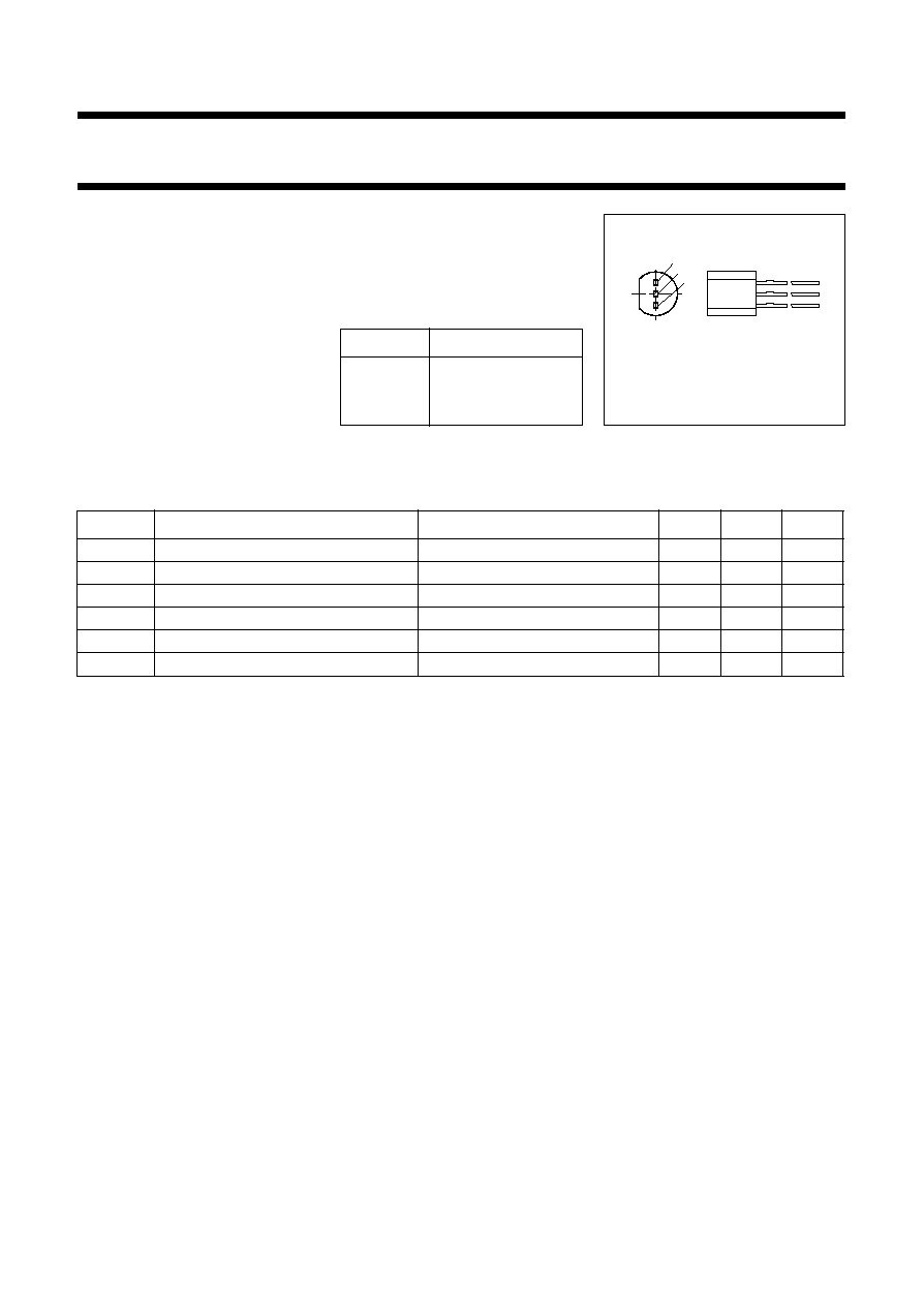
PINNING
PIN
DESCRIPTION
1
base
2
collector
3
emitter
Fig.1 Simplified outline SOT54.
1
3
2
MSB033
QUICK REFERENCE DATA
SYMBOL
PARAMETER
CONDITIONS
TYP.
MAX.
UNIT
V
CEO
collector-emitter voltage
open base
-
18
V
I
C
collector current (DC)
-
150
mA
P
tot
total power dissipation
up to T
s
= 60
∞
C; see Fig.2
-
1.9
W
f
T
transition frequency
I
C
= 100 mA; V
CE
= 10 V; see Fig.4
4
-
GHz
C
re
feedback capacitance
I
C
= 0; V
CE
= 10 V; see Fig.5
1.2
-
pF
T
j
junction temperature
-
175
∞
C

1995 Sep 26
3
Philips Semiconductors
Product specification
NPN video transistor
BFQ131
LIMITING VALUES
In accordance with the Absolute Maximum Rating System (IEC 134).
Note
1. T
s
= the temperature at the soldering point of the collector pin.
SYMBOL
PARAMETER
CONDITIONS
MIN.
MAX.
UNIT
V
CBO
collector-base voltage
open emitter
-
25
V
V
CEO
collector-emitter voltage
open base
-
18
V
V
EBO
emitter-base voltage
open collector
-
2
V
I
C
collector current (DC)
-
150
mA
P
tot
total power dissipation
up to T
s
= 60
∞
C; note 1; see Fig.2
-
1.9
W
T
stg
storage temperature
-
65
+150
∞
C
T
j
junction temperature
-
175
∞
C
Fig.2 Power derating curve.
handbook, halfpage
0
50
100
200
150
2
1.5
0.5
0
1
MBG315
Ptot
(W)
Ts (
o
C)

1995 Sep 26
4
Philips Semiconductors
Product specification
NPN video transistor
BFQ131
THERMAL CHARACTERISTICS
Note
1. T
s
= the temperature at the soldering point of the collector pin.
CHARACTERISTICS
T
j
= 25
∞
C unless otherwise specified.
SYMBOL
PARAMETER
CONDITIONS
VALUE
UNIT
R
th j-s
thermal resistance from junction to
soldering point
up to T
s
= 60
∞
C; note 1; P
tot
= 1.9 W
60
K/W
SYMBOL
PARAMETER
CONDITIONS
MIN.
TYP.
MAX.
UNIT
V
(BR)CBO
collector-base breakdown voltage
I
C
= 0.1 mA; I
E
= 0
25
-
-
V
V
(BR)CEO
collector-emitter breakdown voltage I
C
= 0.1 mA; I
B
= 0
18
-
-
V
V
(BR)EBO
emitter-base breakdown voltage
I
E
= 0.1 mA; I
C
= 0
2
-
-
V
I
CES
collector-emitter cut-off current
V
CE
= 18 V; V
BE
= 0
-
-
1
µ
A
h
FE
DC current gain
I
C
= 25 mA; V
CE
= 10 V;
see Fig.3
25
-
f
T
transition frequency
I
C
= 100 mA; V
CE
= 10 V;
f = 500 MHz; see Fig.4
-
4
-
GHz
C
re
feedback capacitance
I
C
= 0; V
CE
= 10 V; f = 1 MHz;
see Fig.5
-
1.2
-
pF
1995 Sep 26
5
Philips Semiconductors
Product specification
NPN video transistor
BFQ131
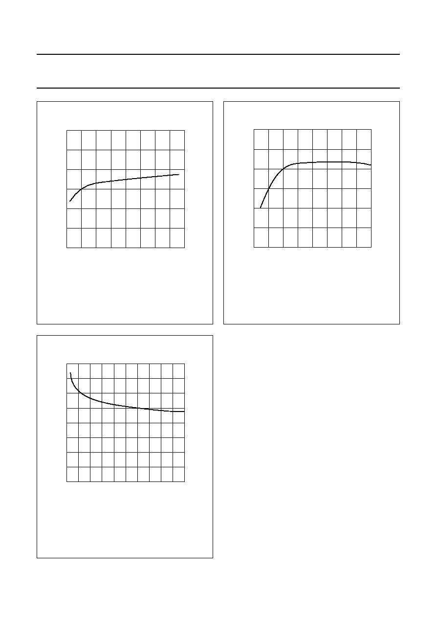
Fig.3
DC current gain as a function of collector
current; typical values.
V
CE
= 10 V; T
j
= 25
∞
C.
handbook, halfpage
0
120
80
40
0
40
80
160
MBB361
120
I (mA)
C
FE
h
Fig.4
Transition frequency as a function of
collector current; typical values.
V
CE
= 10 V; f = 500 MHz; T
j
= 25
∞
C.
handbook, halfpage
0
6
4
2
0
50
MBG317
100
150
200
fT
(MHz)
IC (mA)
Fig.5
Feedback capacitance as a function of
collector-emitter voltage; typical values.
f = 1 MHz; I
C
= 0; T
j
= 25
∞
C.
handbook, halfpage
0
4
20
2
1.5
0.5
0
1
MBG316
8
12
16
Cre
(pF)
VCE (V)