
DATA SHEET
Product specification
File under Discrete Semiconductors, SC14
September 1995
DISCRETE SEMICONDUCTORS
BFQ149
PNP 5 GHz wideband transistor
September 1995
2
Philips Semiconductors
Product specification
PNP 5 GHz wideband transistor
BFQ149
DESCRIPTION
PNP transistor in a SOT89 envelope.
It is intended for use in
UHF applications such as broadband
aerial amplifiers (30 to 860 MHz) and
in microwave amplifiers such as radar
systems, spectrum analyzers, etc.,
using SMD technology.
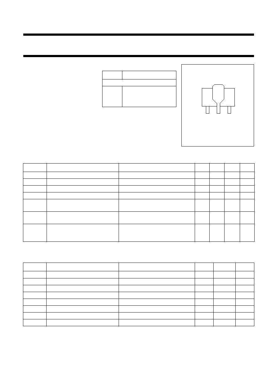
PINNING
PIN
DESCRIPTION
Code: FG
1
emitter
2
collector
3
base
Fig.1 SOT89.
fpage
1
2
3
Bottom view
MBK514
QUICK REFERENCE DATA
LIMITING VALUES
In accordance with the Absolute Maximum System (IEC 134).
Note
1. T
s
is the temperature at the soldering point of the collector tab.
SYMBOL
PARAMETER
CONDITIONS
MIN.
TYP.
MAX.
UNIT
V
CEO
collector-emitter voltage
open base
-
-
-
15
V
I
C
DC collector current
-
-
-
100
mA
P
tot
total power dissipation
up to T
s
= 135
�
C (note 1)
-
-
1
W
h
FE
DC current gain
I
C
=
-
70 mA; V
CE
=
-
10 V; T
j
= 25
�
C 20
50
-
f
T
transition frequency
I
C
=
-
75 mA; V
CE
=
-
10 V;
f = 500 MHz; T
j
= 25
�
C
4
5
-
GHz
G
UM
maximum unilateral power gain
I
C
=
-
50 mA; V
CE
=
-
10 V;
f = 500 MHz; T
amb
= 25
�
C
-
12
-
dB
F
noise figure
I
C
=
-
50 mA; V
CE
=
-
10 V;
R
s
= 60
;
f = 500 MHz;
T
amb
= 25
�
C
-
3.75
-
dB
SYMBOL
PARAMETER
CONDITIONS
MIN.
MAX.
UNIT
V
CBO
collector-base voltage
open emitter
-
-
20
V
V
CEO
collector-emitter voltage
open base
-
-
15
V
V
EBO
emitter-base voltage
open collector
-
-
3
V
I
C
DC collector current
-
-
100
mA
I
CM
peak collector current
f
>
1 MHz
-
-
150
mA
P
tot
total power dissipation
up to T
s
= 135
�
C (note 1)
-
1
W
T
stg
storage temperature
-
65
150
�
C
T
j
junction temperature
-
150
�
C
September 1995
3
Philips Semiconductors
Product specification
PNP 5 GHz wideband transistor
BFQ149
THERMAL RESISTANCE
Note
1. T
s
is the temperature at the soldering point of the collector tab.
CHARACTERISTICS
T
j
= 25
�
C unless otherwise specified.
Note
1. G
UM
is the maximum unilateral power gain, assuming S
12
is zero and
SYMBOL
PARAMETER
CONDITIONS
THERMAL RESISTANCE
R
th j-s
thermal resistance from junction to
soldering point
up to T
s
= 135
�
C (note 1)
40 K/W
SYMBOL
PARAMETER
CONDITIONS
MIN. TYP. MAX.
UNIT
I
CBO
collector cut-off current
I
E
= 0; V
CB
=
-
10 V;
-
-
100
nA
h
FE
DC current gain
I
C
=
-
70 mA; V
CE
=
-
10 V
20
50
-
f
T
transition frequency
I
C
=
-
70 mA; V
CE
=
-
10 V;
f = 500 MHz; T
amb
= 25
�
C
4
5
-
GHz
C
c
collector capacitance
I
E
= 0; V
CB
=
-
10 V; f = 1 MHz
-
2
-
pF
C
e
emitter capacitance
I
C
= 0; V
EB
=
-
0.5 V; f = 1 MHz
-
4
-
pF
C
re
feedback capacitance
I
C
= 0; V
CE
=
-
10 V; f = 1 MHz
-
1.7
-
pF
G
UM
maximum unilateral power gain
(note 1)
I
C
=
-
50 mA; V
CE
=
-
10 V;
f = 500 MHz; T
amb
= 25
�
C
-
12
-
dB
F
noise figure
I
C
=
-
50 mA; V
CE
=
-
10 V;
R
s
= 60
;
f = 500 MHz;
T
amb
= 25
�
C
-
3.75
-
dB
G
UM
10
S
21
2
1
S
11
2
�
1
S
22
2
�
--------------------------------------------------------------
dB.
log
=
September 1995
4
Philips Semiconductors
Product specification
PNP 5 GHz wideband transistor
BFQ149
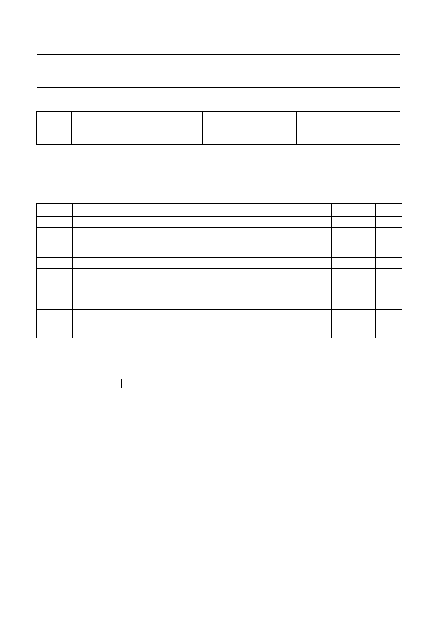
Fig.2
Collector capacitance as a function of
collector-base voltage.
I
E
= 0; f = 1 MHz; T
j
= 25
�
C.
handbook, halfpage
MEA328
0
20
4
0
3
10
2
1
C c
(pF)
VCB (V)
Fig.3
Transition frequency as a function of
collector current.
V
CE
=
-
10 V; f = 500 MHz; T
amb
= 25
�
C.
handbook, halfpage
0
50
100
8
6
2
0
4
MBB347
(GHz)
T
f
I (mA)
C
Fig.4
DC current gain as a function of collector
current.
V
CE
=
-
10 V; T
j
= 25
�
C.
handbook, halfpage
MBB345
0
80
60
20
0
100
200
FE
h
40
I (mA)
C
Fig.5
Maximum unilateral power gain as a
function of frequency.
I
c
=
-
50 mA; V
CE
=
-
10 V; T
amb
= 25
�
C.
handbook, halfpage
40
0
20
30
10
MEA329
10
2
10
3
10
4
10
f (MHz)
G UM
(dB)
September 1995
5
Philips Semiconductors
Product specification
PNP 5 GHz wideband transistor
BFQ149
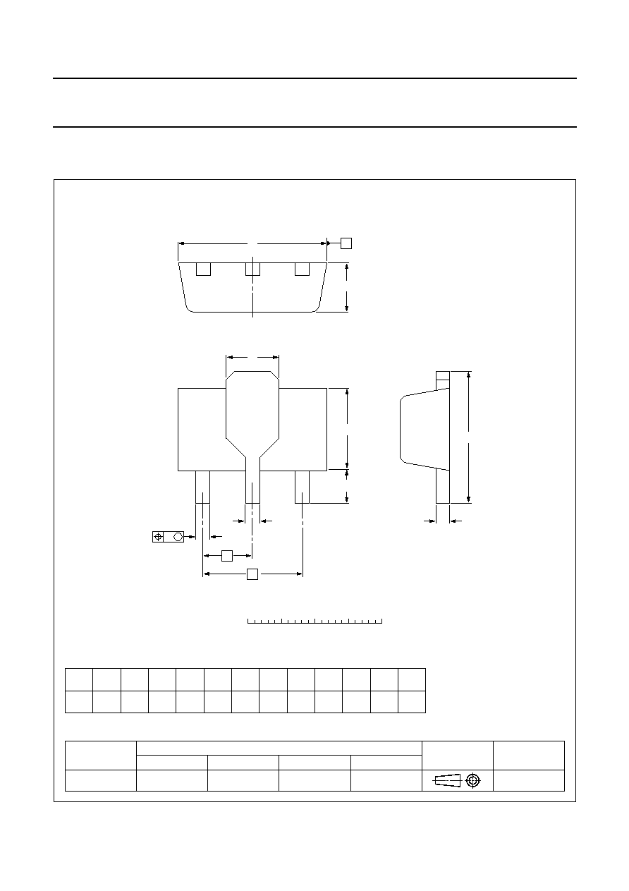
PACKAGE OUTLINE
REFERENCES
OUTLINE
VERSION
EUROPEAN
PROJECTION
ISSUE DATE
IEC
JEDEC
EIAJ
DIMENSIONS (mm are the original dimensions)
SOT89
97-02-28
w
M
e
1
e
E
HE
B
0
2
4 mm
scale
b3
b2
b1
c
D
L
A
Plastic surface mounted package; collector pad for good heat transfer; 3 leads
SOT89
1
2
3
UNIT
A
mm
1.6
1.4
0.48
0.35
c
0.44
0.37
D
4.6
4.4
E
2.6
2.4
HE
4.25
3.75
e
3.0
w
0.13
e1
1.5
L
min.
0.8
b2
b1
0.53
0.40
b3
1.8
1.4