/home/web/doc/html/philips/167228

DATA SHEET
Product specification
File under Discrete Semiconductors, SC14
September 1995
DISCRETE SEMICONDUCTORS
BFQ17
NPN 1 GHz wideband transistor
September 1995
2
Philips Semiconductors
Product specification
NPN 1 GHz wideband transistor
BFQ17
DESCRIPTION
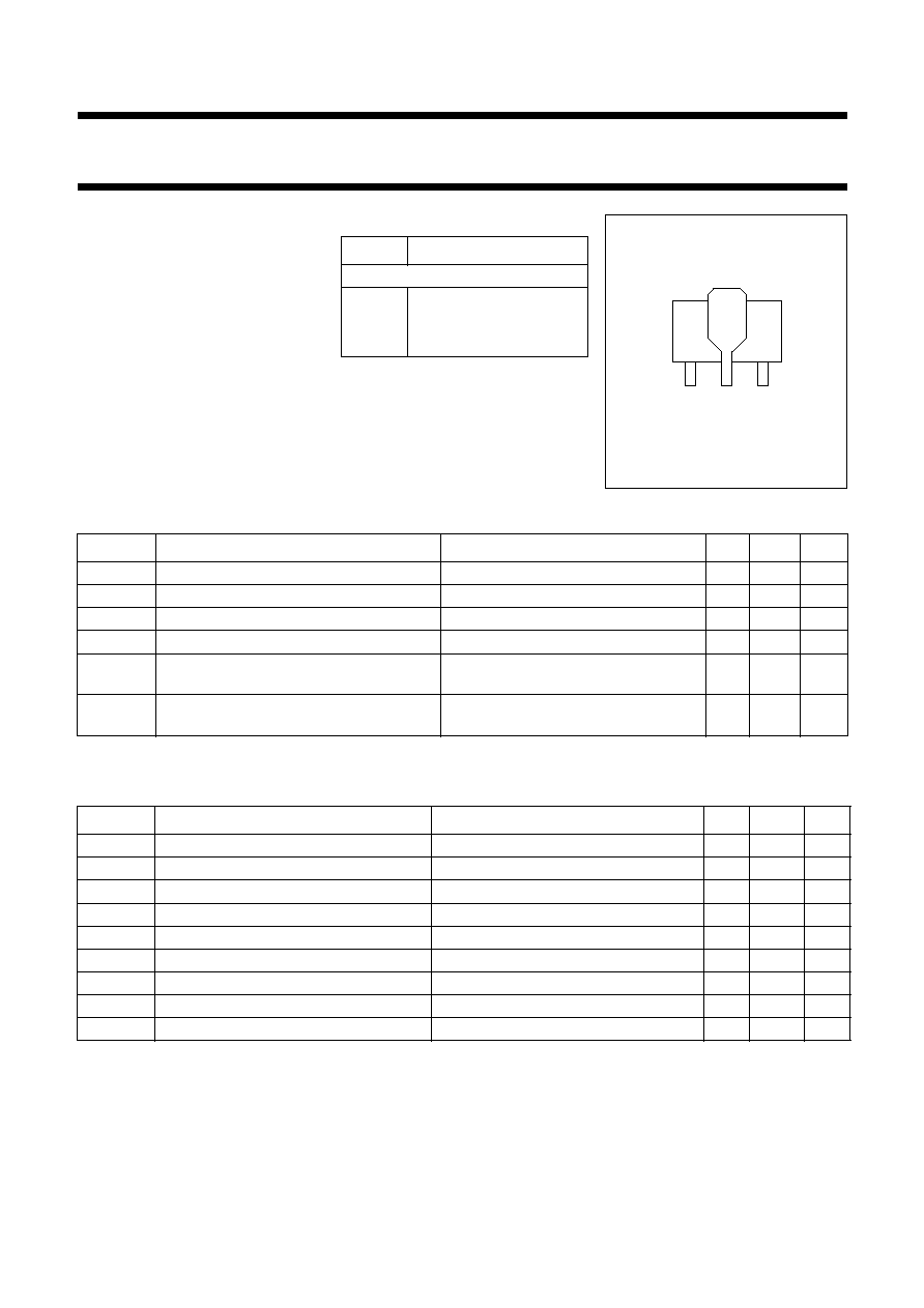
NPN transistor in a SOT89 plastic
envelope intended for application in
thick and thin-film circuits. The
transistor has extremely good
intermodulation properties and a high
power gain.
PINNING
PIN
DESCRIPTION
Code: FA
1
emitter
2
collector
3
base
Fig.1 SOT89.
page
1
2
3
Bottom view
MBK514
QUICK REFERENCE DATA
LIMITING VALUES
In accordance with the Absolute Maximum System (IEC 134).
Note
1. T
s
is the temperature at the soldering point of the collector tab.
SYMBOL
PARAMETER
CONDITIONS
TYP. MAX.
UNIT
V
CBO
collector-base voltage
open emitter
-
40
V
V
CEO
collector-emitter voltage
open base
-
25
V
I
CM
peak collector current
-
300
mA
P
tot
total power dissipation
up to T
s
= 145
�
C (note 1)
-
1
W
f
T
transition frequency
I
C
= 150 mA; V
CE
= 15 V; f = 500 MHz;
T
j
= 25
�
C
1.5
-
GHz
C
re
feedback capacitance
I
C
= 10 mA; V
CE
= 15 V; f = 1 MHz;
T
amb
= 25
�
C
1.9
-
pF
SYMBOL
PARAMETER
CONDITIONS
MIN.
MAX.
UNIT
V
CBO
collector-base voltage
open emitter
-
40
V
V
CER
collector-emitter voltage
R
BE
50
-
40
V
V
CEO
collector-emitter voltage
open base
-
25
V
V
EBO
emitter-base voltage
open collector
-
2
V
I
C
DC collector current
-
150
mA
I
CM
peak collector current
f
>
1 MHz
-
300
mA
P
tot
total power dissipation
up to T
s
= 145
�
C (note 1)
-
1
W
T
stg
storage temperature
-
65
150
�
C
T
j
junction temperature
-
175
�
C
September 1995
3
Philips Semiconductors
Product specification
NPN 1 GHz wideband transistor
BFQ17
THERMAL RESISTANCE
Note
1. T
s
is the temperature at the soldering point of the collector tab.
CHARACTERISTICS
T
j
= 25
�
C unless otherwise specified.
Note
1. G
UM
is the maximum unilateral power gain, assuming S
12
is zero and
SYMBOL
PARAMETER
CONDITIONS
THERMAL RESISTANCE
R
th j-s
thermal resistance from junction to
soldering point
up to T
s
= 145
�
C (note 1)
30 K/W
SYMBOL
PARAMETER
CONDITIONS
MIN. TYP. MAX.
UNIT
I
CBO
collector cut-off current
I
E
= 0; V
CB
= 20 V; T
j
= 50
�
C
-
-
20
�
A
V
CE sat
collector-emitter saturation voltage
I
C
= 100 mA; I
B
= 10 mA
-
-
0.5
V
h
FE
DC current gain
I
C
= 150 mA; V
CE
= 5 V
25
80
-
C
c
collector capacitance
I
E
= i
e
= 0; V
CB
= 15 V; f = 1 MHz
-
-
4
pF
C
re
feedback capacitance
I
C
= 10 mA; V
CE
= 15 V;
f = 1 MHz; T
amb
= 25
�
C
-
1.9
-
pF
f
T
transition frequency
I
C
= 150 mA; V
CE
= 15 V;
f = 500 MHz
-
1.5
-
GHz
G
UM
maximum unilateral power gain
(note 1)
I
C
= 60 mA; V
CE
= 15 V;
f = 200 MHz; T
amb
= 25
�
C
-
16
-
dB
I
C
= 60 mA; V
CE
= 15 V;
f = 800 MHz; T
amb
= 25
�
C
-
6.5
-
dB
G
UM
10
S
21
2
1
S
11
2
�
1
S
22
2
�
--------------------------------------------------------------
dB.
log
=
September 1995
4
Philips Semiconductors
Product specification
NPN 1 GHz wideband transistor
BFQ17
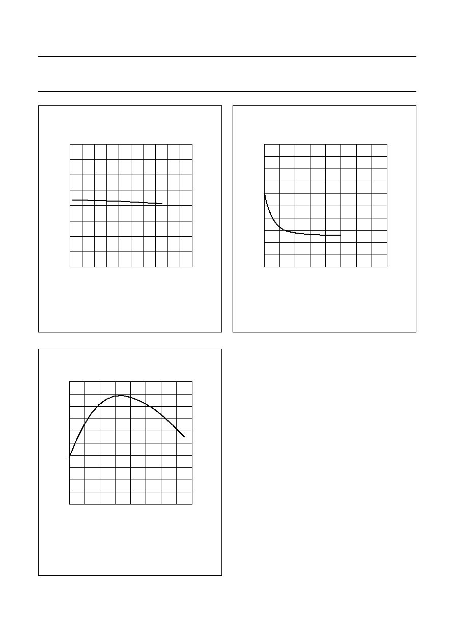
Fig.2
DC current gain as a function of collector
current.
V
CE
= 5 V; T
j
= 25
�
C.
handbook, halfpage
MBB365
0
160
120
40
0
100
200
I (mA)
C
FE
h
80
I
E
= i
e
= 0; f = 1 MHz; T
j
= 25
�
C.
Fig.3
Collector capacitance as a function of
collector-base voltage.
handbook, halfpage
0
10
20
10
0
8
MBB828
30
6
4
2
C c
(pF)
VCB (V)
40
Fig.4
Transition frequency as a function of
collector current.
V
CE
= 15 V; f = 500 MHz; T
j
= 25
�
C.
handbook, halfpage
MBB364
0
40
80
160
2
1.6
0.8
0
1.2
120
I (mA)
C
(GHz)
T
f
0.4
September 1995
5
Philips Semiconductors
Product specification
NPN 1 GHz wideband transistor
BFQ17
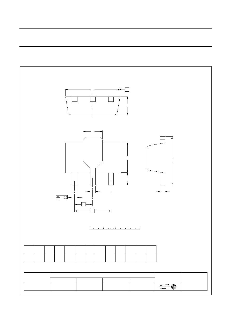
PACKAGE OUTLINE
REFERENCES
OUTLINE
VERSION
EUROPEAN
PROJECTION
ISSUE DATE
IEC
JEDEC
EIAJ
DIMENSIONS (mm are the original dimensions)
SOT89
97-02-28
w
M
e
1
e
E
HE
B
0
2
4 mm
scale
b3
b2
b1
c
D
L
A
Plastic surface mounted package; collector pad for good heat transfer; 3 leads
SOT89
1
2
3
UNIT
A
mm
1.6
1.4
0.48
0.35
c
0.44
0.37
D
4.6
4.4
E
2.6
2.4
HE
4.25
3.75
e
3.0
w
0.13
e1
1.5
L
min.
0.8
b2
b1
0.53
0.40
b3
1.8
1.4