 | –≠–ª–µ–∫—Ç—Ä–æ–Ω–Ω—ã–π –∫–æ–º–ø–æ–Ω–µ–Ω—Ç: BFQ221 | –°–∫–∞—á–∞—Ç—å:  PDF PDF  ZIP ZIP |
DATA SHEET
Product specification
Supersedes data of 1996 July 18
File under Discrete Semiconductors, SC05
1996 Sep 04
DISCRETE SEMICONDUCTORS
BFQ221
NPN video transistor
1996 Sep 04
2
Philips Semiconductors
Product specification
NPN video transistor
BFQ221
APPLICATIONS
∑
Primarily intended for buffer stages
in high resolution colour monitors.
DESCRIPTION
NPN silicon transistor encapsulated
in a 3-lead plastic SOT54 package.
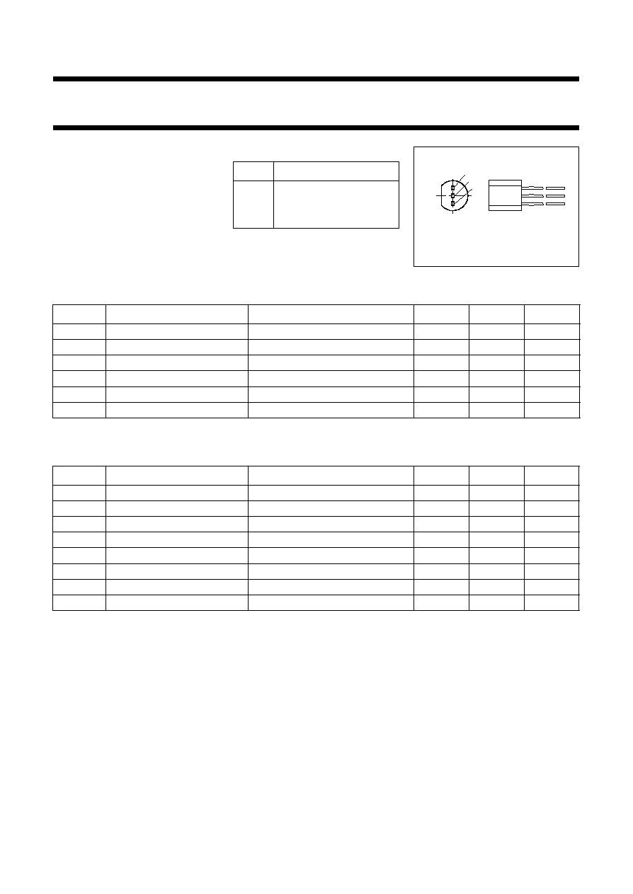
PINNING
PIN
DESCRIPTION
1
base
2
collector
3
emitter
Fig.1 Simplified outline SOT54.
1
3
2
MSB033
QUICK REFERENCE DATA
LIMITING VALUES
In accordance with the Absolute Maximum Rating System (IEC 134).
Note
1. T
s
is the temperature at the soldering point of the collector pin.
SYMBOL
PARAMETER
CONDITIONS
TYP
MAX
UNIT
V
CBO
collector-base voltage
open emitter
-
100
V
I
C
collector current (DC)
-
100
mA
P
tot
total power dissipation
up to T
s
= 60
∞
C
-
1.15
W
f
T
transition frequency
I
C
= 25 mA; V
CE
= 10 V
1
-
GHz
C
re
feedback capacitance
I
C
= 0; V
CB
= 10 V
1.7
-
pF
T
j
junction temperature
-
150
∞
C
SYMBOL
PARAMETER
CONDITIONS
MIN
MAX
UNIT
V
CBO
collector-base voltage
open emitter
-
100
V
V
CER
collector-emitter voltage
R
BE
= 100
-
95
V
V
EBO
emitter-base voltage
open collector
-
3
V
I
C
collector current (DC)
see Fig.2
-
100
mA
I
C(AV)
average collector current
see Fig.2
-
100
mA
P
tot
total power dissipation
up to T
s
= 60
∞
C; note 1; see Fig.3
-
1.15
W
T
stg
storage temperature
-
65
+150
∞
C
T
j
junction temperature
-
150
∞
C
1996 Sep 04
3
Philips Semiconductors
Product specification
NPN video transistor
BFQ221
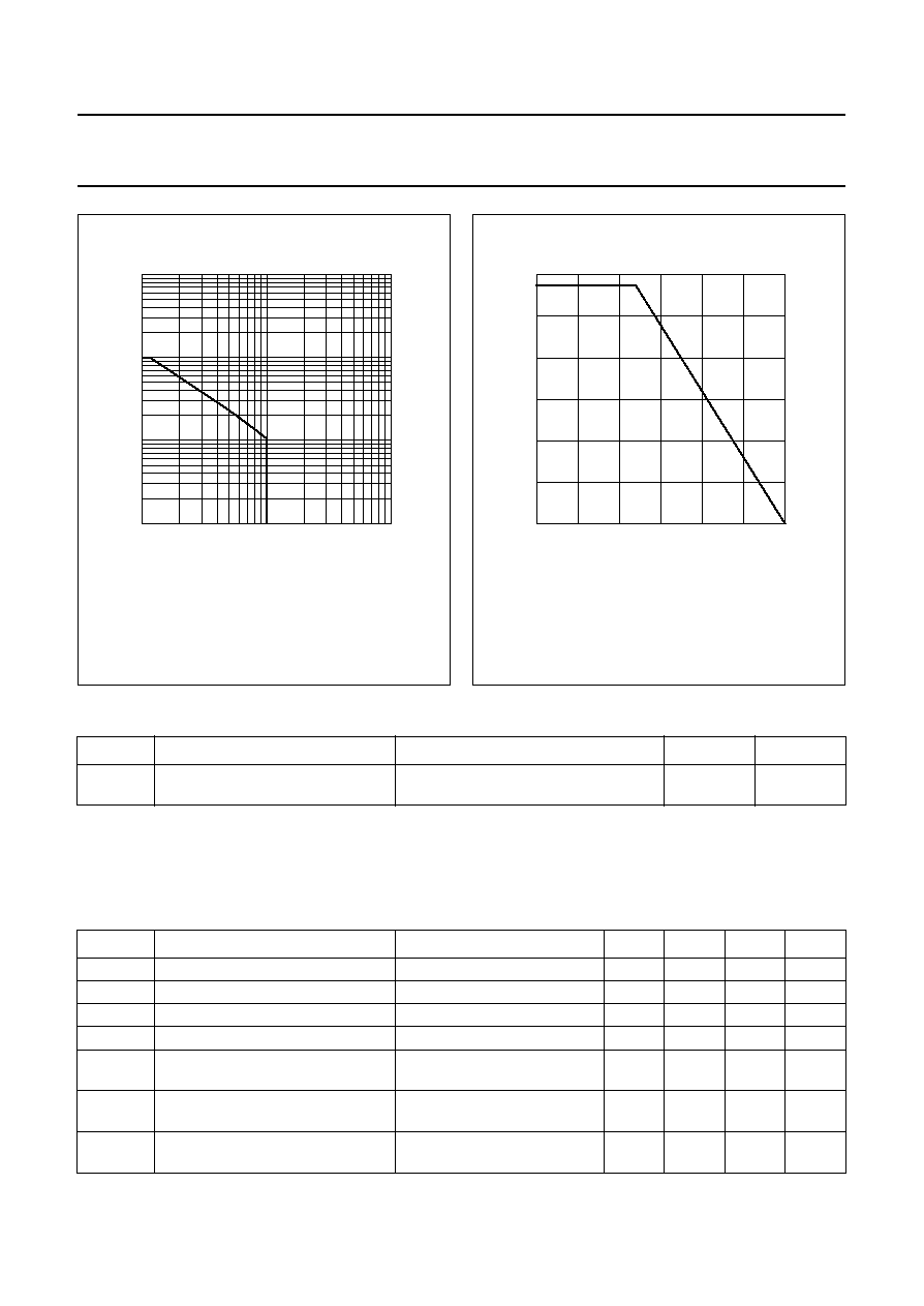
handbook, halfpage
MBG476
10
2
10
10
2
10
3
10
3
10
1
VCE (V)
IC
(mA)
Fig.2 DC SOAR.
handbook, halfpage
0
1.2
0.8
Ptot
(W)
0.4
0
50
100
150
Ts (
o
C)
MBG477
Fig.3 Power derating curve.
THERMAL CHARACTERISTICS
Note
1. T
s
is the temperature of the soldering point of the collector pin.
CHARACTERISTICS
T
j
= 25
∞
C unless otherwise specified.
SYMBOL
PARAMETER
CONDITIONS
VALUE
UNIT
R
th j-s
thermal resistance from junction to
soldering point
P
tot
= 1.15 W; up to T
s
= 60
∞
C; note 1
78
K/W
SYMBOL
PARAMETER
CONDITIONS
MIN
TYP
MAX
UNIT
V
(BR)CBO
collector-base breakdown voltage
I
C
= 0.1 mA; I
E
= 0
100
-
-
V
V
(BR)CER
collector-emitter breakdown voltage I
C
= 1 mA; R
BE
= 100
95
-
-
V
V
(BR)EBO
emitter-base breakdown voltage
I
C
= 0; I
E
= 0.1 mA
3
-
-
V
I
CES
collector-emitter leakage current
V
CE
= 50 V; V
BE
= 0
-
-
100
µ
A
h
FE
DC current gain
I
C
= 25 mA; V
CE
= 10 V;
see Fig.4
20
-
-
f
T
transition frequency
I
C
= 25 mA; V
CE
= 10 V;
f = 500 MHz; see Fig.5
-
1
-
GHz
C
re
feedback capacitance
I
C
= 0; V
CB
= 10 V; f = 1 MHz;
see Fig.6
-
1.7
-
pF
1996 Sep 04
4
Philips Semiconductors
Product specification
NPN video transistor
BFQ221
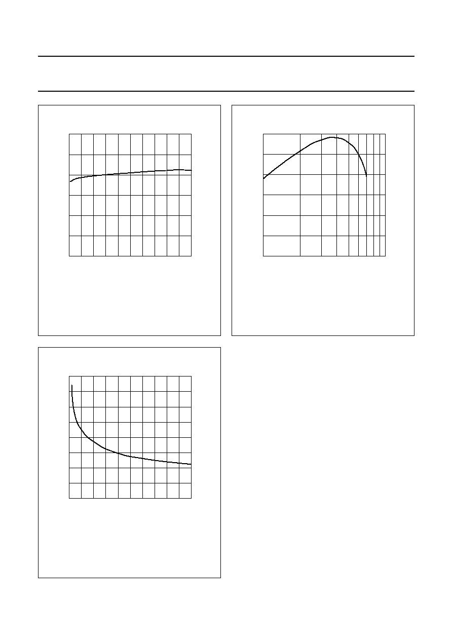
handbook, halfpage
0
20
100
hFE
60
20
0
40
MBG478
40
60
80
IC (mA)
Fig.4
DC current gain as a function of collector
current; typical values.
V
CE
= 10 V; t
p
= 500
µ
s.
handbook, halfpage
0
0.4
0.8
1.2
10
2
MBG479
10
IC (mA)
20
50
fT
(MHz)
Fig.5
Transition frequency as a function of
collector current; typical values.
V
CE
= 10 V; f = 500 MHz.
handbook, halfpage
0
2
10
Cre
(pF)
3
1
0
2
4
MBG480
4
6
8
VCB (V)
Fig.6
Feedback capacitance as a function of
collector-base voltage; typical values.
f = 1 MHz.
1996 Sep 04
5
Philips Semiconductors
Product specification
NPN video transistor
BFQ221
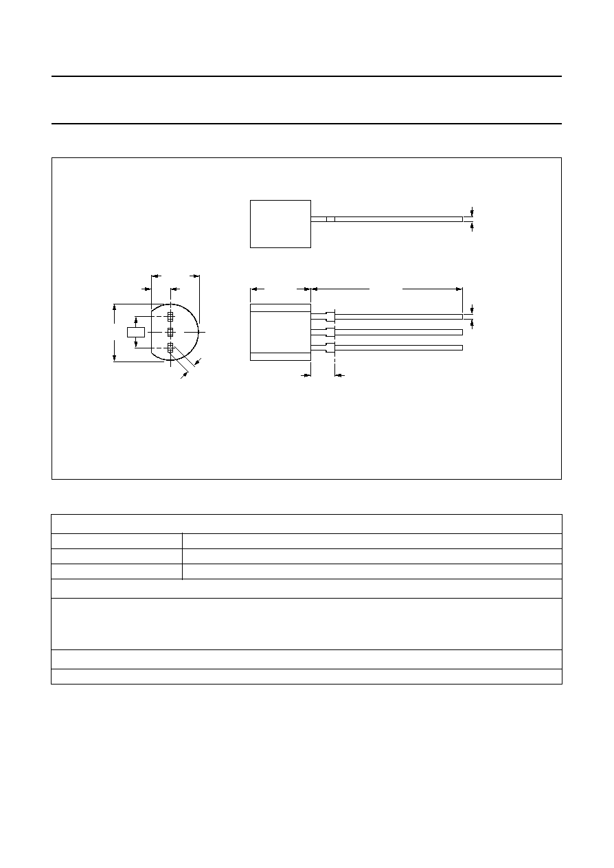
PACKAGE OUTLINE
DEFINITIONS
LIFE SUPPORT APPLICATIONS
These products are not designed for use in life support appliances, devices, or systems where malfunction of these
products can reasonably be expected to result in personal injury. Philips customers using or selling these products for
use in such applications do so at their own risk and agree to fully indemnify Philips for any damages resulting from such
improper use or sale.
Data Sheet Status
Objective specification
This data sheet contains target or goal specifications for product development.
Preliminary specification
This data sheet contains preliminary data; supplementary data may be published later.
Product specification
This data sheet contains final product specifications.
Limiting values
Limiting values given are in accordance with the Absolute Maximum Rating System (IEC 134). Stress above one or
more of the limiting values may cause permanent damage to the device. These are stress ratings only and operation
of the device at these or at any other conditions above those given in the Characteristics sections of the specification
is not implied. Exposure to limiting values for extended periods may affect device reliability.
Application information
Where application information is given, it is advisory and does not form part of the specification.
Fig.7 SOT54.
Dimensions in mm.
andbook, full pagewidth
MBC014 - 1
2.54
4.8
max
4.2 max
1.7
1.4
0.66
0.56
1
2
3
5.2 max
12.7 min
2.0 max
(1)
0.48
0.40
0.40
min