 | –≠–ª–µ–∫—Ç—Ä–æ–Ω–Ω—ã–π –∫–æ–º–ø–æ–Ω–µ–Ω—Ç: BFQ540 | –°–∫–∞—á–∞—Ç—å:  PDF PDF  ZIP ZIP |

DATA SHEET
Product specification
Supersedes data of 1995 Sep 04
File under Discrete Semiconductors, SC14
1998 Aug 27
DISCRETE SEMICONDUCTORS
BFQ540
NPN wideband dual transistor
book, halfpage
M3D109
1998 Aug 27
2
Philips Semiconductors
Product specification
NPN wideband dual transistor
BFQ540
FEATURES
∑
High gain
∑
High output voltage
∑
Low noise
∑
Gold metallization ensures
excellent reliability
∑
Low thermal resistance.
APPLICATIONS
∑
VHF, UHF and CATV amplifiers.
DESCRIPTION
NPN wideband dual transistor in a
plastic SOT89 package.
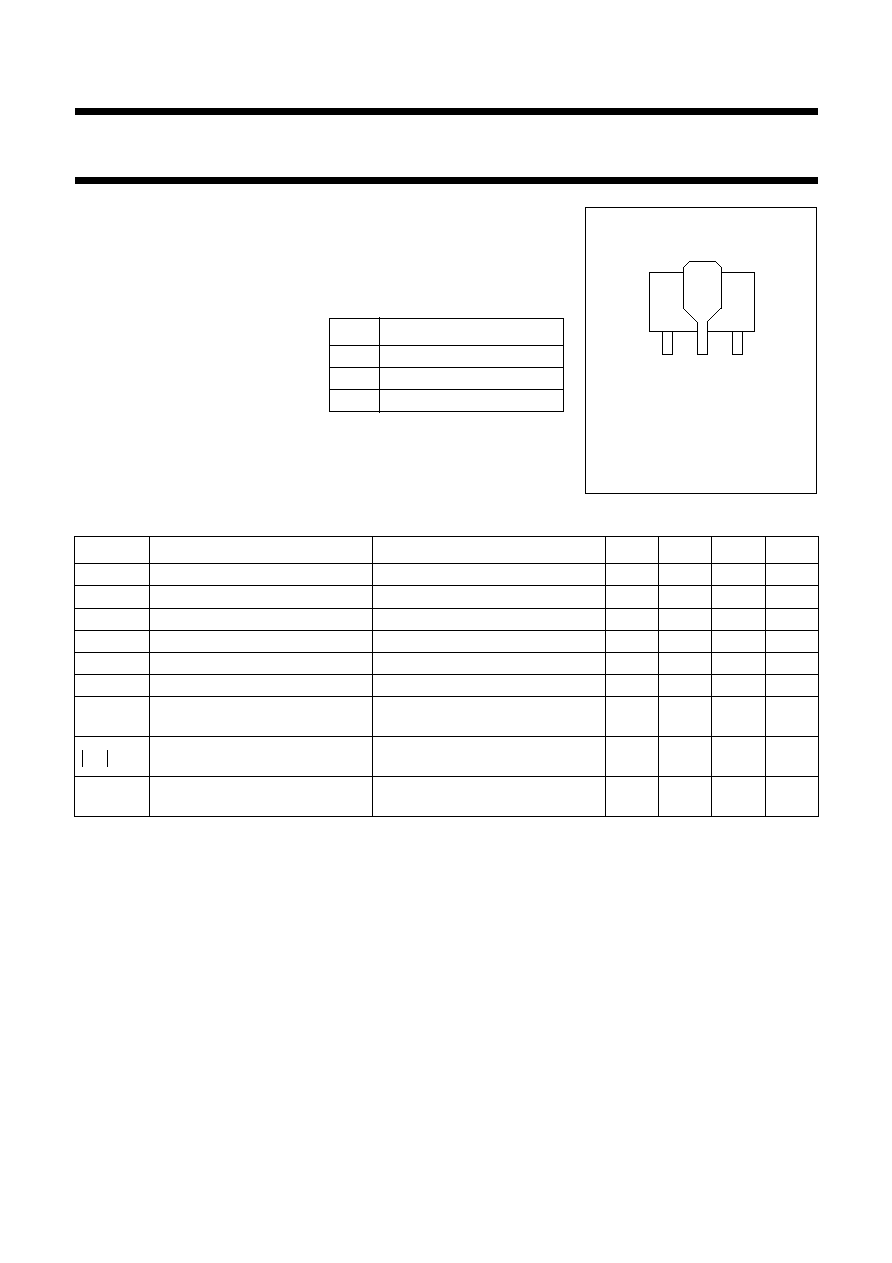
PINNING
PIN
DESCRIPTION
1
emitter
2
collector
3
base
Fig.1 SOT89.
Marking code: N4.
page
1
2
3
Bottom view
MBK514
QUICK REFERENCE DATA
Note
1. T
s
is the temperature at the soldering point of the collector pin.
SYMBOL
PARAMETER
CONDITIONS
MIN.
TYP.
MAX.
UNIT
V
CBO
collector-base voltage
open emitter
-
-
20
V
V
CES
collector-emitter voltage
R
BE
= 0
-
-
15
V
V
EBO
collector-base voltage
open collector
-
-
2
V
I
C
collector current (DC)
-
-
120
mA
P
tot
total power dissipation
T
s
60
∞
C; note 1
-
-
1.2
W
h
FE
DC current gain
I
C
= 40 mA; V
CE
= 8 V; T
j
= 25
∞
C
60
120
250
f
T
transition frequency
I
C
= 40 mA; V
CE
= 8 V; f = 1 GHz;
T
amb
= 25
∞
C
-
9
-
GHz
insertion power gain
I
C
= 40 mA; V
CE
= 8 V;
f = 900 MHz; T
amb
= 25
∞
C
12
13
-
dB
F
noise figure
I
C
= 40 mA; V
CE
= 8 V;
f = 900 MHz;
S
=
opt
-
1.9
2.4
dB
S
21
2
1998 Aug 27
3
Philips Semiconductors
Product specification
NPN wideband dual transistor
BFQ540
LIMITING VALUES
In accordance with the Absolute Maximum Rating System (IEC 134).
THERMAL CHARACTERISTICS
SYMBOL
PARAMETER
CONDITIONS
MIN.
MAX.
UNIT
V
CBO
collector-base voltage
open emitter
-
20
V
V
CES
collector-emitter voltage
R
BE
= 0
-
15
V
V
EBO
emitter-base voltage
open collector
-
2
V
I
C
collector current (DC)
-
120
mA
P
tot
total power dissipation
T
s
60
∞
C
-
1.2
W
T
stg
storage temperature
-
65
+150
∞
C
T
j
operating junction temperature
-
175
∞
C
SYMBOL
PARAMETER
CONDITIONS
VALUE
UNIT
R
th j-s
thermal resistance from junction
to soldering point
T
s
60
∞
C; P
tot
= 1.2 W
95
K/W
Fig.2 Power derating curve.
V
CE
9 V.
0
50
100
200
0.8
0
MBG241
150
1.0
1.2
0.2
0.4
0.6
Ptot
(W)
Tj (
o
C)
1.4
Fig.3 SOAR.
handbook, halfpage
MBG244
10
2
10
10
10
2
1
10
3
IC
(mA)
VCE (V)
1998 Aug 27
4
Philips Semiconductors
Product specification
NPN wideband dual transistor
BFQ540
CHARACTERISTICS
T
j
= 25
∞
C unless otherwise specified.
Notes
1. d
im
=
-
60 dB (DIN45004B); V
CE
= 8 V; I
C
= 40 mA; R
L
= 50
;
V
p
= V
o
; V
q
= V
o
-
6 dB; V
r
= V
o
-
6 dB;
f
p
= 795.25 MHz; f
q
= 803.25 MHz; f
r
= 805.5 MHz;
measured at f
p
+ f
q
-
f
r
= 793.25 MHz.
2. d
im
=
-
60 dB (DIN 45004B); I
C
= 40 mA; V
CE
= 8 V; R
L
= 50
;
V
p
= V
q
= V
o
; f
p
= 806 MHz; f
q
= 810 MHz;
measured at 2f
p
-
f
q
= 802 MHz.
3. I
C
= 40 mA; V
CE
= 8 V; R
L
= 50
;
V
p
= V
q
= 225 mV; f
p
= 250 MHz; f
q
= 560 MHz;
measured at f
p
+ f
q
= 810 MHz.
SYMBOL
PARAMETER
CONDITIONS
MIN.
TYP.
MAX.
UNIT
V
(BR)CBO
collector-base breakdown voltage
open emitter; I
C
= 10
µ
A; I
E
= 0
20
-
-
V
V
(BR)CES
collector-emitter breakdown voltage R
BE
= 0; I
C
= 40
µ
A
15
-
-
V
V
(BR)EBO
emitter-base breakdown voltage
I
E
= 100
µ
A; I
C
= 0
2
-
-
V
I
CBO
collector-base leakage current
V
CB
= 8 V; I
E
= 0
-
-
50
nA
I
EBO
emitter-base leakage current
V
CB
= 1 V; I
C
= 0
-
-
200
nA
h
FE
DC current gain
I
C
= 40 mA; V
CE
= 8 V
60
120
250
f
T
transition frequency
I
C
= 40 mA; V
CE
= 8 V;
f
m
= 1 GHz
-
9
-
GHz
C
e
emitter capacitance
I
C
= i
e
= 0; V
EB
= 0.5 V; f = 1 MHz
-
2
-
pF
C
re
feedback capacitance
I
C
= 0; V
CE
= 8 V; f = 1 MHz
-
0.9
-
pF
insertion power gain
I
C
= 40 mA; V
CE
= 8 V;
f = 900 MHz; T
amb
= 25
∞
C
12
13
-
dB
V
o
output voltage
note 1
-
500
-
mV
note 2
-
350
-
mV
d
2
second order intermodulation
distortion
note 3
-
-
-
53
dB
F
noise figure
I
C
= 40 mA; V
CE
= 8 V;
f = 900 MHz;
S
=
opt
-
1.9
2.4
dB
S
21
2

1998 Aug 27
5
Philips Semiconductors
Product specification
NPN wideband dual transistor
BFQ540
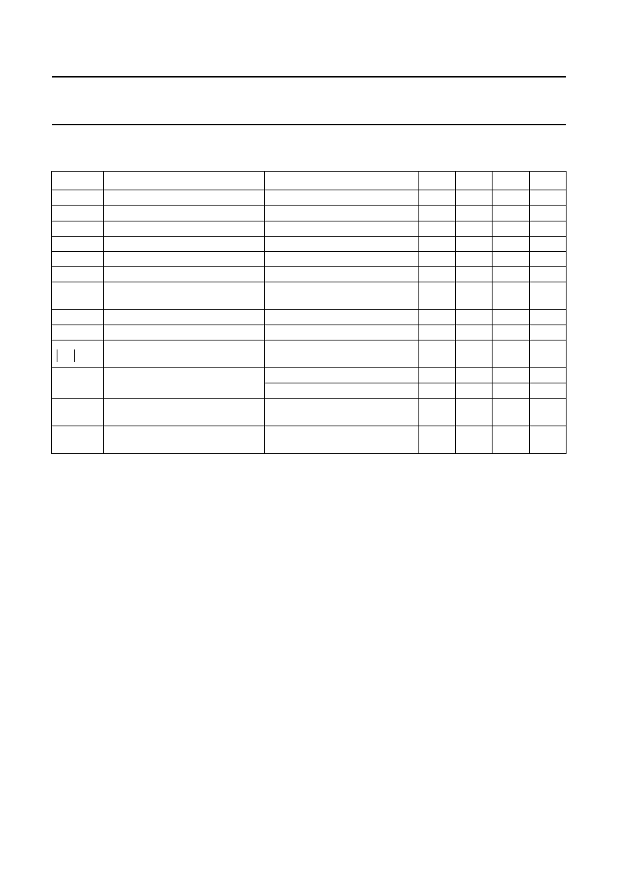
Fig.4
Feedback capacitance as a function of
collector-base voltage; typical values.
I
C
= 0; f = 1 MHz.
handbook, halfpage
MRA688
1.0
0.8
0.6
0.4
0.2
0
0
4
8
12
Cre
(pF)
VCB (V)
Fig.5
Transition frequency as a function of
collector current; typical values.
f = 1 GHz; T
amb
= 25
∞
C.
handbook, halfpage
MRA689
fT
(GHz)
IC (mA)
12
8
4
0
10
-
1
1
10
10
2
VCE = 8V
VCE = 4V
Fig.6
Intermodulation distortion as a function of
collector current; typical values.
V
CE
= 8 V; V
o
= 475 mV; R
L
= 50
.
f
p
+ f
q
-
f
r
= 793.25 MHz; T
amb
= 25
∞
C.
handbook, halfpage
10
60
20
70
60
MBG242
50
40
30
20
30
40
50
dim
(dB)
IC (mA)
Fig.7
Second order intermodulation distortion as
a function of collector current; typical values.
V
CE
= 8 V; V
o
= 225 mV; R
L
= 50
; f
p
+ f
q
= 810 MHz; T
amb
= 25
∞
C.
handbook, halfpage
10
60
MBG243
20
30
40
50
20
70
60
50
40
30
d2
(dB)
IC (mA)