 | –≠–ª–µ–∫—Ç—Ä–æ–Ω–Ω—ã–π –∫–æ–º–ø–æ–Ω–µ–Ω—Ç: BFQ621 | –°–∫–∞—á–∞—Ç—å:  PDF PDF  ZIP ZIP |
DATA SHEET
Product specification
Supersedes data of 1995 Apr 11
File under Discrete Semiconductors, SC14
1995 Sep 26
DISCRETE SEMICONDUCTORS
BFQ621
NPN 7 GHz wideband transistor
1995 Sep 26
2
Philips Semiconductors
Product specification
NPN 7 GHz wideband transistor
BFQ621
FEATURES
∑
High power gain
∑
High output voltage
∑
High maximum junction temperature
∑
Gold metallization ensures excellent reliability.
APPLICATIONS
It is primarily intended for use in MATV and microwave
amplifiers, such as aerial amplifiers, radar systems,
oscilloscopes, spectrum analyzers, etc.
DESCRIPTION
Silicon NPN transistor in a 4-lead dual-emitter SOT172A2
package with a ceramic cap. All leads are isolated from the
mounting base. Emitter ballasting resistors and application
of gold sandwich metallization ensures an optimum
temperature profile and excellent reliability properties.
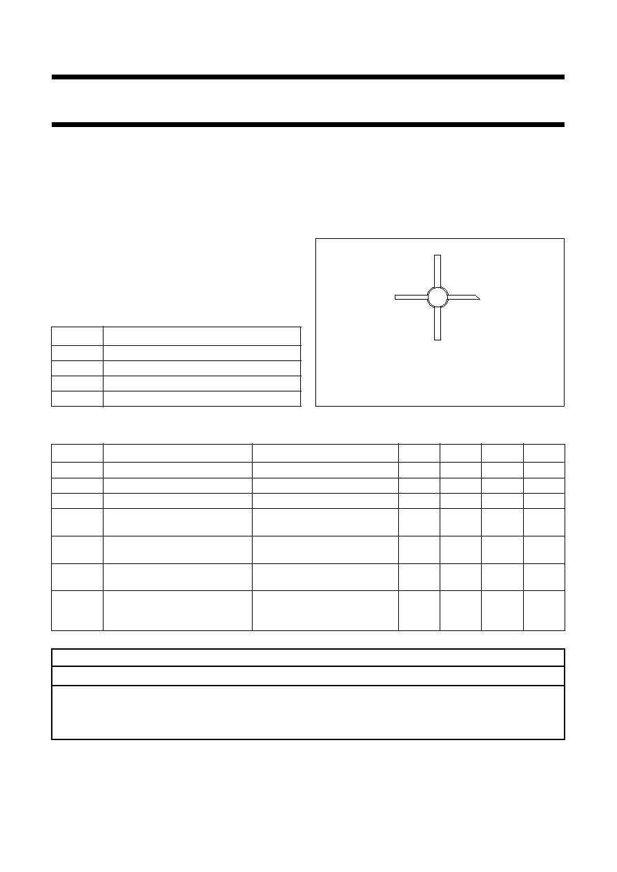
PINNING
PIN
DESCRIPTION
1
collector
2
emitter
3
base
4
emitter
Fig.1 SOT172A2.
handbook, halfpage
MSA457
4
2
3
1
Top view
QUICK REFERENCE DATA
SYMBOL
PARAMETER
CONDITIONS
MIN.
TYP.
MAX.
UNIT
V
CEO
collector-emitter voltage
open base
-
-
16
V
I
C
collector current (DC)
-
-
150
mA
P
tot
total power dissipation
up to T
mb
= 25
∞
C
-
-
8
W
h
FE
DC current gain
I
C
= 120 mA; V
CE
= 18 V;
T
amb
= 25
∞
C
40
-
-
f
T
transition frequency
I
C
= 120 mA; V
CE
= 18 V;
f = 1 GHz; T
amb
= 25
∞
C
-
7
-
GHz
G
UM
maximum unilateral power gain
I
C
= 120 mA; V
CE
= 18 V;
f = 500 MHz; T
amb
= 25
∞
C
-
18.5
-
dB
V
O
output voltage
I
C
= 120 mA; V
CE
= 18 V;
f
(p + q
-
r)
= 793.25 MHz;
d
im
=
-
60 dB; R
L
= 75
-
1.2
-
V
WARNING
Product and environmental safety - toxic materials
This product contains beryllium oxide. The product is entirely safe provided that the BeO disc is not damaged.
All persons who handle, use or dispose of this product should be aware of its nature and of the necessary safety
precautions. After use, dispose of as chemical or special waste according to the regulations applying at the location of
the user. It must never be thrown out with the general or domestic waste.
1995 Sep 26
3
Philips Semiconductors
Product specification
NPN 7 GHz wideband transistor
BFQ621
LIMITING VALUES
In accordance with the Absolute Maximum Rating System (IEC 134).
THERMAL CHARACTERISTICS
SYMBOL
PARAMETER
CONDITIONS
MIN.
MAX.
UNIT
V
CBO
collector-base voltage
open emitter
-
25
V
V
CEO
collector-emitter voltage
open base
-
16
V
V
EBO
emitter-base voltage
open collector
-
2
V
I
C
collector current (DC)
-
150
mA
P
tot
total power dissipation
up to T
mb
= 25
∞
C
-
8
W
T
stg
storage temperature
-
65
+175
∞
C
T
j
junction temperature
-
+200
∞
C
SYMBOL
PARAMETER
CONDITIONS
VALUE
UNIT
R
th j-mb
thermal resistance from junction to mounting base P
tot
= 8 W; up to T
mb
= 25
∞
C
21.9
K/W
1995 Sep 26
4
Philips Semiconductors
Product specification
NPN 7 GHz wideband transistor
BFQ621
CHARACTERISTICS
T
j
= 25
∞
C (unless otherwise specified).
Notes
1. G
UM
is the maximum unilateral power gain, assuming s
12
is zero.
2. d
im
=
-
60dB (DIN45004B); see Fig.2; I
C
= 120 mA; V
CE
= 18 V; R
L
= 75
; T
amb
= 25
∞
C;
V
p
= V
O
; f
p
= 445.25 MHz;
V
q
= V
O
-
6 dB; f
q
= 453.25 MHz;
V
r
= V
O
-
6 dB; f
r
= 455.25 MHz;
measured at f
(p + q
-
r)
= 443.25 MHz; see Fig.5.
3. d
im
=
-
60dB (DIN45004B); see Fig.2; I
C
= 120 mA; V
CE
= 18 V; R
L
= 75
; T
amb
= 25
∞
C;
V
p
= V
O
; f
p
= 795.25 MHz;
V
q
= V
O
-
6 dB; f
q
= 803.25 MHz;
V
r
= V
O
-
6 dB; f
r
= 805.25 MHz;
measured at f
(p + q
-
r)
= 793.25 MHz; see Fig.6.
4. V
O
= 50 dBmV = 316 mV; I
C
= 90 mA; V
CE
= 18 V; R
L
= 75
; T
amb
= 25
∞
C;
measured at f
(p + q)
= 450 MHz; see Fig.7.
5. V
O
= 50 dBmV = 316 mV; I
C
= 90 mA; V
CE
= 18 V; R
L
= 75
; T
amb
= 25
∞
C;
measured at f
(p + q)
= 810 MHz; see Fig.8.
SYMBOL
PARAMETER
CONDITIONS
MIN.
TYP.
MAX.
UNIT
V
(BR)CBO
collector-base breakdown voltage
I
C
= 0.1 mA; I
E
= 0
-
-
25
V
V
(BR)CEO
collector-emitter breakdown voltage I
C
= 10 mA; I
B
= 0
-
-
16
V
V
(BR)EBO
emitter-base breakdown voltage
I
E
= 0.1 mA; I
C
= 0
-
-
2
V
I
CBO
collector-base leakage current
I
E
= 0; V
CB
= 18 V
-
-
100
µ
A
h
FE
DC current gain
I
C
= 50 mA; V
CE
= 10 V
50
-
160
f
T
transition frequency
I
C
= 120 mA; V
CE
= 18 V;
f = 1 GHz; see Fig.3
-
7
-
GHz
C
c
collector capacitance
I
E
= i
e
= 0; V
CB
= 18 V;
f = 1 MHz
-
1.5
-
pF
C
e
emitter capacitance
I
C
= i
c
= 0; V
EB
= 0.5 V;
f = 1 MHz
-
5
-
pF
C
re
feedback capacitance
I
C
= 0; V
CE
= 18 V; f = 1 MHz;
see Fig.4
-
0.85
1.2
pF
G
UM
maximum unilateral power gain;
note 1
I
C
= 120 mA; V
CE
= 18 V;
f = 500 MHz; T
amb
= 25
∞
C;
-
18.5
-
dB
I
C
= 120 mA; V
CE
= 18 V;
f = 800 MHz; T
amb
= 25
∞
C;
-
14.5
-
dB
V
O
output voltage
note 2
-
1.35
-
V
note 3
-
1.2
-
V
d
2
second order intermodulation
distortion
note 4
-
-
60
-
dB
note 5
-
-
60
-
dB
G
UM
10
s
21
2
1
s
11
2
≠
(
)
1
s
22
2
≠
(
)
------------------------------------------------------------ dB.
log
=
1995 Sep 26
5
Philips Semiconductors
Product specification
NPN 7 GHz wideband transistor
BFQ621
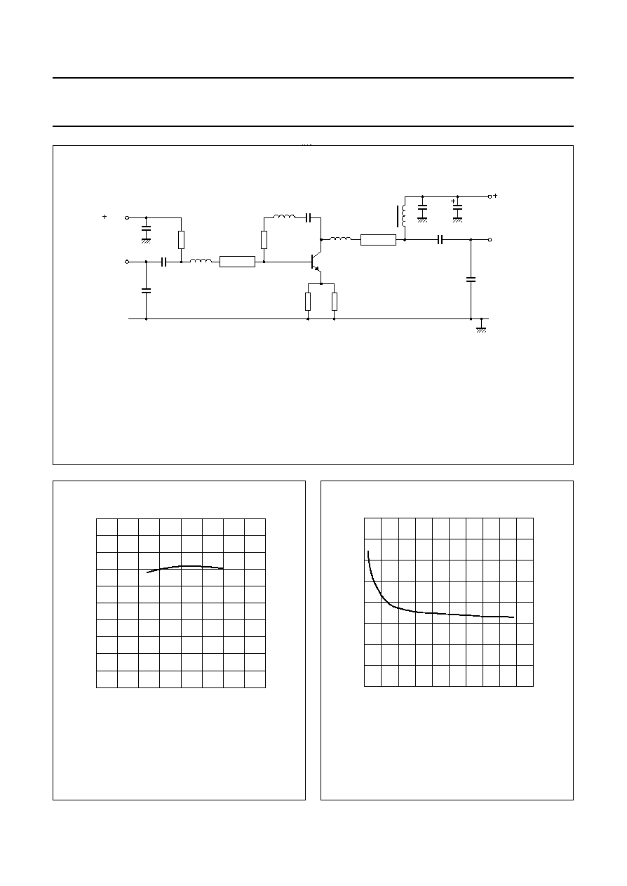
Fig.2 Intermodulation distortion and second order distortion MATV test circuit.
L1 = 8 nH.
L2 = 15 nH, 2 turns copper wire, internal diameter 2 mm.
L3 = 10 nH, 2 turns copper wire, internal diameter 1.5 mm.
L5: Lp = 21 mm; Rc = 75
.
L6: Lp = 16 mm; Rc = 75
.
MEA260
handbook, full pagewidth
MEA260
DUT
VBB
10 k
10 nF
1 pF
L5
input
75
240
L2
33
33
L3
10 nF
1 pF
10 nF
L4
output
75
VCC
L1
10 nF
L6
4.7
µ
F
10 nF
Fig.3
Transition frequency as a function
of collector current; typical values.
V
CE
= 18 V; f = 1 GHz.
handbook, halfpage
0
100
200
50
150
10
6
8
2
0
4
MLC991
(GHz)
T
f
I (mA)
C
Fig.4
Feedback capacitance as a function of
collector-base voltage; typical values.
I
C
= 0; f = 1 MHz.
handbook, halfpage
MLC990
0
2.0
1.5
1.0
0.5
0
5
10
15
20
25
V (V)
CB
C re
(pF)