 | –≠–ª–µ–∫—Ç—Ä–æ–Ω–Ω—ã–π –∫–æ–º–ø–æ–Ω–µ–Ω—Ç: BFQ67/T1 | –°–∫–∞—á–∞—Ç—å:  PDF PDF  ZIP ZIP |

DATA SHEET
Product specification
File under Discrete Semiconductors, SC14
September 1995
DISCRETE SEMICONDUCTORS
BFQ67
NPN 8 GHz wideband transistor
September 1995
2
Philips Semiconductors
Product specification
NPN 8 GHz wideband transistor
BFQ67
FEATURES
∑
High power gain
∑
Low noise figure
∑
High transition frequency
∑
Gold metallization ensures
excellent reliability.
DESCRIPTION
Silicon NPN transistor in a plastic
SOT23 envelope. It is designed for
wideband applications such as
satellite TV tuners and RF portable
communications equipment up to
2 GHz.
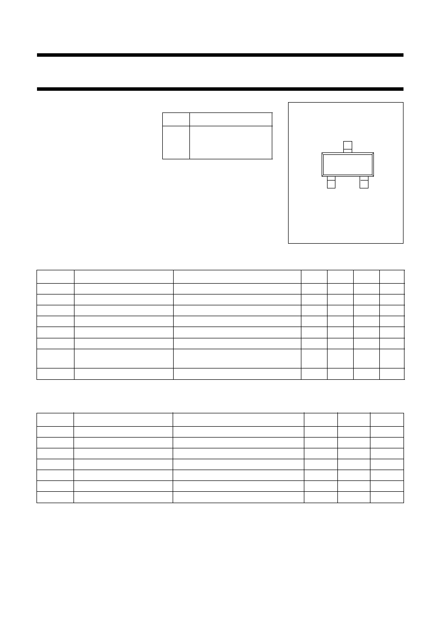
PINNING
PIN
DESCRIPTION
1
base
2
emitter
3
collector
Fig.1 SOT23.
alfpage
MSB003
Top view
1
2
3
QUICK REFERENCE DATA
LIMITING VALUES
In accordance with the Absolute Maximum System (IEC 134).
Note
1. T
s
is the temperature at the soldering point of the collector tab.
SYMBOL
PARAMETER
CONDITIONS
MIN.
TYP.
MAX.
UNIT
V
CBO
collector-base voltage
open emitter
-
-
20
V
V
CEO
collector-emitter voltage
open base
-
-
10
V
I
C
DC collector current
-
-
50
mA
P
tot
total power dissipation
up to T
s
= 97
∞
C; note 1
-
-
300
mW
h
FE
DC current gain
I
C
= 15 mA; V
CE
= 5 V
60
100
-
f
T
transition frequency
I
C
= 15 mA; V
CE
= 8 V
-
8
-
GHz
G
UM
maximum unilateral
power gain
I
C
= 15 mA; V
CE
= 8 V;
f = 1 GHz
-
14
-
dB
F
noise figure
I
C
= 5 mA; V
CE
= 8 V; f = 1 GHz
-
1.3
-
dB
SYMBOL
PARAMETER
CONDITIONS
MIN.
MAX.
UNIT
V
CBO
collector-base voltage
open emitter
-
20
V
V
CEO
collector-emitter voltage
open base
-
10
V
V
EBO
emitter-base voltage
open collector
-
2.5
V
I
C
DC collector current
-
50
mA
P
tot
total power dissipation
up to T
s
= 97
∞
C; note 1
-
300
mW
T
stg
storage temperature range
-
65
150
∞
C
T
j
junction temperature
-
175
∞
C
September 1995
3
Philips Semiconductors
Product specification
NPN 8 GHz wideband transistor
BFQ67
THERMAL RESISTANCE
Note
1. T
s
is the temperature at the soldering point of the collector tab.
CHARACTERISTICS
T
j
= 25
∞
C unless otherwise specified.
Note
1. G
UM
is the maximum unilateral power gain, assuming S
12
is zero and
SYMBOL
PARAMETER
THERMAL RESISTANCE
R
th j-s
from junction to soldering point (note 1)
260 K/W
SYMBOL
PARAMETER
CONDITIONS
MIN.
TYP.
MAX.
UNIT
I
CBO
collector cut-off current
I
E
= 0; V
CB
= 5 V
-
-
50
nA
h
FE
DC current gain
I
C
= 15 mA; V
CE
= 5 V
60
100
-
C
c
collector capacitance
I
E
= i
e
= 0; V
CB
= 8 V; f = 1 MHz
-
0.7
-
pF
C
e
emitter capacitance
I
C
= i
c
= 0; V
EB
= 0.5 V; f = 1 MHz
-
1.3
-
pF
C
re
feedback capacitance
I
C
= 0; V
CB
= 8 V; f = 1 MHz
-
0.5
-
pF
f
T
transition frequency
I
C
= 15 mA; V
CE
= 8 V
-
8
-
GHz
G
UM
maximum unilateral
power gain (note 1)
I
C
= 15 mA; V
CE
= 8 V;
T
amb
= 25
∞
C; f = 1 GHz
-
14
-
dB
I
C
= 15 mA; V
CE
= 8 V; f = 2 GHz
-
8
-
dB
F
noise figure
s
=
opt
; I
C
= 5 mA; V
CE
= 8 V;
T
amb
= 25
∞
C; f = 1 GHz
-
1.3
-
dB
s
=
opt
; I
C
= 15 mA; V
CE
= 8 V;
T
amb
= 25
∞
C; f = 1 GHz
-
1.7
-
dB
s
=
opt
; I
C
= 5 mA; V
CE
= 8 V;
T
amb
= 25
∞
C; f = 2 GHz
-
2.2
-
dB
I
C
= 5 mA; V
CE
= 8 V;
T
amb
= 25
∞
C; f = 2 GHz; Z
s
= 60
-
2.5
-
dB
s
=
opt
; I
C
= 15 mA; V
CE
= 8 V;
T
amb
= 25
∞
C; f = 2 GHz
-
2.7
-
dB
I
C
= 15 mA; V
CE
= 8 V;
T
amb
= 25
∞
C; f = 2 GHz; Z
s
= 60
-
3
-
dB
G
UM
10 log
S
21
2
1
S
11
2
≠
1
S
22
2
≠
--------------------------------------------------------------
dB.
=
September 1995
4
Philips Semiconductors
Product specification
NPN 8 GHz wideband transistor
BFQ67
Fig.2 Power derating curve.
handbook, halfpage
0
50
100
200
400
300
100
0
200
150
MRA614
Ptot
(mW)
Ts (
oC)
Fig.3
DC current gain as a function of collector
current, typical values.
V
CE
= 5 V.
handbook, halfpage
0
120
80
40
0
20
40
MBB301
60
I (mA)
C
FE
h
Fig.4
Feedback capacitance as a function of
collector-base voltage, typical values.
I
C
= i
c
= 0; f = 1 MHz.
handbook, halfpage
0
5
10
15
VCB (V)
Cre
(pF)
0.8
0.6
0.2
0
0.4
MRA607
Fig.5
Transition frequency as a function of
collector current, typical values.
V
CE
= 8 V; T
amb
= 25
∞
C; f = 2 GHz.
handbook, halfpage
0
10
20
40
8
6
2
0
4
MBB303
30
I (mA)
C
(GHz)
T
f
10
September 1995
5
Philips Semiconductors
Product specification
NPN 8 GHz wideband transistor
BFQ67
In Figs 6 to 9, G
UM
= maximum unilateral power gain;
MSG = maximum stable gain; G
max
= maximum available
gain.
Fig.6
Gain as a function of collector current,
typical values.
V
CE
= 8 V; f = 1 GHz.
handbook, halfpage
0
10
IC (mA)
20
30
25
0
20
15
gain
(dB)
10
5
MRA611
MSG
GUM
Gmax
Fig.7
Gain as a function of frequency, typical
values.
V
CE
= 8 V; I
C
= 5 mA.
handbook, halfpage
50
gain
(dB)
0
10
MRA610
10
2
10
3
10
4
10
20
30
f (MHz)
40
MSG
GUM
Gmax
Fig.8
Gain as a function of frequency, typical
values.
V
CE
= 8 V; I
C
= 15 mA.
handbook, halfpage
50
gain
(dB)
0
10
MRA608
10
2
10
3
10
4
10
20
30
f (MHz)
40
Gmax
GUM
MSG
Fig.9
Gain as a function of frequency, typical
values.
V
CE
= 8 V; I
C
= 30 mA.
handbook, halfpage
50
gain
(dB)
0
10
MRA609
10
2
10
3
10
4
10
20
30
f (MHz)
40
Gmax
GUM
MSG