Philips Semiconductors
Product specification
74ABT16543
74ABTH16543
16-bit latched transceivers with dual enable
(3-State)
2
1998 Feb 27
853-1739 19026
FEATURES
∑
Two 8-bit octal transceivers with D-type latch
∑
Live insertion/extraction permitted
∑
Power-up 3-State
∑
Power-up reset
∑
Multiple V
CC
and GND pins minimize switching noise
∑
Back-to-back registers for storage
∑
Separate controls for data flow in each direction
∑
74ABTH16543 incorporates bus-hold data inputs which eliminate
the need for external pull-up resistors to hold unused inputs
∑
Output capability: +64mA/≠32mA
∑
Latch-up protection exceeds 500mA per JEDEC Std 17
∑
ESD protection exceeds 2000V per MIL STD 883 Method 3015
and 200V per Machine Model
∑
See 74ABT161543 for same function with Master Reset control
pins
DESCRIPTION
The 74ABT16543 high-performance BiCMOS device combines low
static and dynamic power dissipation with high speed and high
output drive.
The 74ABT16543 16-bit registered transceiver contains two sets of
D-type latches for temporary storage of data flowing in either
direction. Separate Latch Enable (nLEAB, nLEBA) and Output
Enable (nOEAB, nOEBA) inputs are provided for each register to
permit independent control of data transfer in either direction. The
outputs are guaranteed to sink 64mA.
Two options are available, 74ABT16543 which does not have the
bus-hold feature and 74ABTH16543 which incorporates the
bus-hold feature.
QUICK REFERENCE DATA
SYMBOL
PARAMETER
CONDITIONS
T
amb
= 25
∞
C; GND = 0V
TYPICAL
UNIT
t
PLH
t
PHL
Propagation delay
nAx to nBx
C
L
= 50pF; V
CC
= 5V
2.5
2.2
ns
C
IN
Input capacitance
V
I
= 0V or V
CC
3
pF
C
I/O
I/O capacitance
V
O
= 0V or V
CC;
3-State
7
pF
I
CCZ
Quiescent supply current
Outputs disabled; V
CC
= 5.5V
550
µ
A
I
CCL
Quiescent su
ly current
Outputs low; V
CC
= 5.5V
9
mA
ORDERING INFORMATION
PACKAGES
TEMPERATURE RANGE
OUTSIDE NORTH AMERICA
NORTH AMERICA
DWG NUMBER
56-Pin Plastic SSOP Type III
≠40
∞
C to +85
∞
C
74ABT16543 DL
BT16543 DL
SOT371-1
56-Pin Plastic TSSOP Type II
≠40
∞
C to +85
∞
C
74ABT16543 DGG
BT16543 DGG
SOT364-1
56-Pin Plastic SSOP Type III
≠40
∞
C to +85
∞
C
74ABTH16543 DL
BH16543 DL
SOT371-1
56-Pin Plastic TSSOP Type II
≠40
∞
C to +85
∞
C
74ABTH16543 DGG
BH16543 DGG
SOT364-1
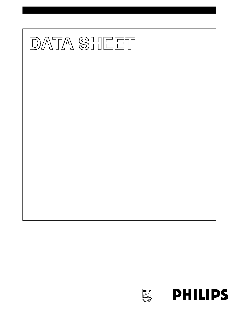
PIN DESCRIPTION
PIN NUMBER
SYMBOL
NAME AND FUNCTION
5, 6, 8, 9, 10, 12, 13, 14
15, 16, 17, 19, 20, 21, 23, 24
1A0 ≠ 1A7,
2A0 ≠ 2A7
Data inputs/outputs
52, 51, 49, 48, 47, 45, 44, 43
42, 41, 40,38, 37, 36, 34, 33
1B0 ≠ 1B7,
2B0 ≠ 2B7
Data inputs/outputs
1, 56
28, 29
1OEAB, 1OEBA,
2OEAB, 2OEBA
A to B / B to A Output Enable inputs (active-Low)
3, 54
26, 31
1EAB, 1EBA,
2EAB, 2EBA
A to B / B to A Enable inputs (active-Low)
2, 55
27, 30
1LEAB, 1LEBA,
2LEAB, 2LEBA
A to B / B to A Latch Enable inputs (active-Low)
4, 11, 18, 25, 32, 39, 46, 53
GND
Ground (0V)
7, 22, 35, 50
V
CC
Positive supply voltage
Philips Semiconductors
Product specification
74ABT16543
74ABTH16543
16-bit latched transceivers with dual enable
(3-State)
1998 Feb 27
4
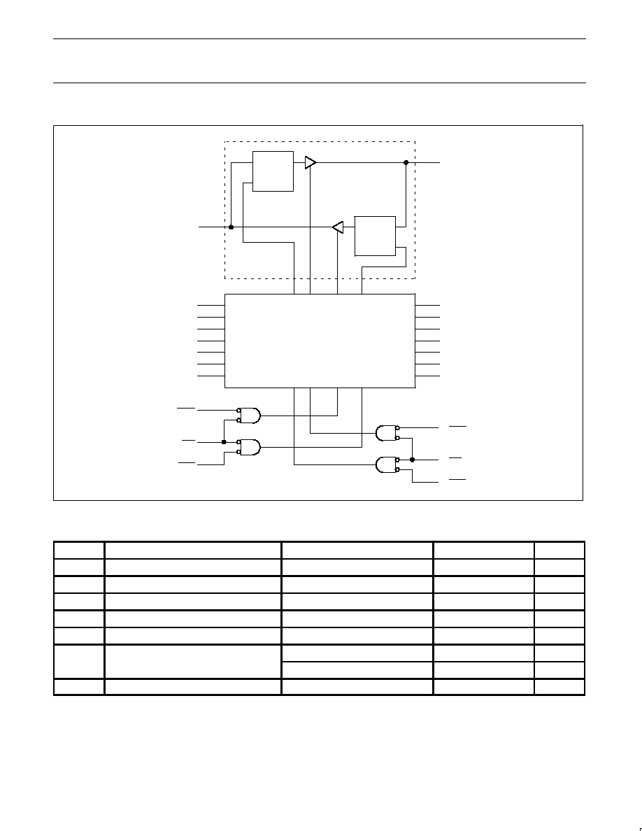
LOGIC SYMBOL
3
54
1EAB
1EBA
2
1LEAB
55
1LEBA
1
1OEAB
56
1OEBA
26
31
2EAB
2EBA
27
2LEAB
30
2LEBA
28
2OEAB
29
2OEBA
5
6
10
12
13
14
8
9
52
51
47
45
44
43
49
48
15
16
20
21
23
24
17
19
42
41
37
36
34
33
40
38
SH00038
1A0 1A1 1A2 1A3 1A4 1A5 1A6 1A7
1B0 1B1 1B2 1B3 1B4 1B5 1B6 1B7
2A0 2A1 2A2 2A3 2A4 2A5 2A6 2A7
2B0 2B1 2B2 2B3 2B4 2B5 2B6 2B7
FUNCTIONAL DESCRIPTION
The 74ABT16543 contains two sets of eight D-type latches, with
separate control pins for each set. Using data flow from A to B as an
example, when the A-to-B Enable (nEAB) input and the A-to-B Latch
Enable (nLEAB) input are Low the A-to-B path is transparent.
A subsequent Low-to-High transition of the nLEAB signal puts the A
data into the latches where it is stored and the B outputs no longer
change with the A inputs. With EAB and nOEAB both Low, the
3-State B output buffers are active and display the data present at
the outputs of the A latches.
Control of data flow from B to A is similar, but using the nEBA,
nLEBA, and nOEBA inputs.
FUNCTION TABLE
INPUTS
OUTPUTS
STATUS
nOEXX
nEXX
nLEXX
nAx or nBx
nBx or nAx
STATUS
H
X
X
X
Z
Disabled
X
H
X
X
Z
Disabled
L
L
L
L
h
l
Z
Z
Disabled + Latch
L
L
L
L
h
l
H
L
Latch + Display
L
L
L
L
L
L
H
L
H
L
Transparent
L
L
H
X
NC
Hold
H = High voltage level
h
= High voltage level one set-up time prior to the Low-to-High transition of nLEXX or nEXX (XX = AB or BA)
L
= Low voltage level
l
= Low voltage level one set-up time prior to the Low-to-High transition of nLEXX or nEXX (XX = AB or BA)
X = Don't care
= Low-to-High transition of nLEXX or nEXX (XX = AB or BA)
NC= No change
Z = High impedance or "off" state
Philips Semiconductors
Product specification
74ABT16543
74ABTH16543
16-bit latched transceivers with dual enable
(3-State)
1998 Feb 27
5
LOGIC DIAGRAM
D
LE
Q
D
LE
Q
DETAIL A
nB0
nB1
nA1
nB2
nA2
nB3
nA3
nB4
nA4
nB5
nA5
nB6
nA6
nB7
nA7
DETAIL A X 7
nOEAB
nEAB
nLEAB
nOEBA
nEBA
nLEBA
nA0
SH00039
ABSOLUTE MAXIMUM RATINGS
1, 2
SYMBOL
PARAMETER
CONDITIONS
RATING
UNIT
V
CC
DC supply voltage
≠0.5 to +7.0
V
I
IK
DC input diode current
V
I
< 0
≠18
mA
V
I
DC input voltage
3
≠1.2 to +7.0
V
I
OK
DC output diode current
V
O
< 0
≠50
mA
V
OUT
DC output voltage
3
output in Off or High state
≠0.5 to +5.5
V
I
O
DC output current
output in Low state
128
mA
I
OUT
DC output current
output in High state
≠64
mA
T
stg
Storage temperature range
≠65 to 150
∞
C
NOTES:
1. Stresses beyond those listed may cause permanent damage to the device. These are stress ratings only and functional operation of the
device at these or any other conditions beyond those indicated under "recommended operating conditions" is not implied. Exposure to
absolute-maximum-rated conditions for extended periods may affect device reliability.
2. The performance capability of a high-performance integrated circuit in conjunction with its thermal environment can create junction
temperatures which are detrimental to reliability. The maximum junction temperature of this integrated circuit should not exceed 150
∞
C.
3. The input and output voltage ratings may be exceeded if the input and output current ratings are observed.