 | –≠–ª–µ–∫—Ç—Ä–æ–Ω–Ω—ã–π –∫–æ–º–ø–æ–Ω–µ–Ω—Ç: BRY39 | –°–∫–∞—á–∞—Ç—å:  PDF PDF  ZIP ZIP |
Document Outline
- FEATURES
- APPLICATIONS
- DESCRIPTION
- PINNING
- QUICK REFERENCE DATA
- LIMITING VALUES
- THERMAL CHARACTERISTICS
- CHARACTERISTICS
- PACKAGE OUTLINE
- DEFINITIONS
- LIFE SUPPORT APPLICATIONS
DATA SHEET
Product specification
Supersedes data of September 1994
File under Discrete Semiconductors, SC04
1997 Jul 24
DISCRETE SEMICONDUCTORS
BRY39
Programmable unijunction
transistor/
Silicon controlled switch
M3D082
1997 Jul 24
2
Philips Semiconductors
Product specification
Programmable unijunction transistor/
Silicon controlled switch
BRY39
FEATURES
∑
Silicon controlled switch
∑
Programmable unijunction
transistor.
APPLICATIONS
∑
Switching applications such as:
≠ Motor control
≠ Oscillators
≠ Relay replacement
≠ Timers
≠ Pulse shapers, etc.
DESCRIPTION
Silicon planar PNPN switch or trigger
device in a TO-72 metal package.
It is an integrated PNP/NPN transistor
pair with all electrodes accessible.
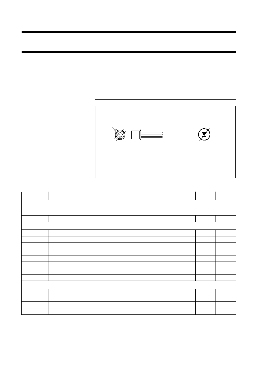
PINNING
PIN
DESCRIPTION
1
cathode
2
cathode gate
3
anode gate (connected to case)
4
anode
handbook, halfpage
MGL168
k
a
kg
ag
Fig.1 Simplified outline (TO-72) and symbol.
book, halfpage
1
2
3
4
MSB028
QUICK REFERENCE DATA
SYMBOL
PARAMETER
CONDITIONS
MAX.
UNIT
Silicon controlled switch
PNP TRANSISTOR
V
EBO
emitter-base voltage
open collector
-
70
V
NPN TRANSISTOR
V
CBO
collector-base voltage
open emitter
70
V
I
ERM
repetitive peak emitter current
-
2.5
A
P
tot
total power dissipation
T
amb
25
∞
C
275
mW
T
j
junction temperature
150
∞
C
V
AK
forward on-state voltage
I
A
= 50 mA; I
AG
= 0; R
KG-K
= 10 k
1.4
V
I
H
holding current
I
AG
= 10 mA; V
BB
=
-
2 V; R
KG-K
= 10 k
1
mA
t
on
turn-on time
0.25
µ
s
t
off
turn-off time
15
µ
s
Programmable unijunction transistor
V
GA
gate-anode voltage
70
V
I
A
anode current (DC)
T
amb
25
∞
C
175
mA
T
j
junction temperature
150
∞
C
I
p
peak point current
V
S
= 10 V; R
G
= 10 k
0.2
µ
A

1997 Jul 24
3
Philips Semiconductors
Product specification
Programmable unijunction transistor/
Silicon controlled switch
BRY39
LIMITING VALUES
In accordance with the Absolute Maximum Rating System (IEC 134).
SYMBOL
PARAMETER
CONDITIONS
MIN.
MAX.
UNIT
P
tot
total power dissipation
T
amb
25
∞
C
-
275
mW
T
stg
storage temperature
-
65
+200
∞
C
T
j
junction temperature
-
150
∞
C
T
amb
operating ambient temperature
-
65
+150
∞
C
Silicon controlled switch
V
CBO
collector-base voltage
open emitter
PNP
-
-
70
V
NPN
-
70
V
V
CER
collector-emitter voltage
R
BE
= 10 k
PNP
-
-
V
NPN
-
70
V
V
CEO
collector-emitter voltage
open base
PNP
-
-
70
V
NPN
-
-
V
V
EBO
emitter-base voltage
open collector
PNP
-
-
70
V
NPN
-
5
V
I
C
collector current (DC)
note 1
PNP
-
-
NPN
-
175
mA
I
CM
peak collector current
note 2
PNP
-
-
NPN
-
175
mA
I
E
emitter current (DC)
PNP
-
175
mA
NPN
-
-
175
mA
I
ERM
repetitive peak emitter current
t
p
= 10
µ
s;
= 0.01
PNP
-
2.5
A
NPN
-
-
2.5
A
Programmable unijunction transistor
V
GA
gate-anode voltage
-
70
V
I
A
anode current (AV)
T
amb
25
∞
C
-
175
mA
1997 Jul 24
4
Philips Semiconductors
Product specification
Programmable unijunction transistor/
Silicon controlled switch
BRY39
Notes
1. Provided the I
E
rating is not exceeded.
2. During switching on, the device can withstand the discharge of a capacitor of a maximum value of 500 pF. This
capacitor is charged when the transistor is in cut-off condition, with a collector supply voltage of 160 V and a series
resistance of 100 k
.
THERMAL CHARACTERISTICS
CHARACTERISTICS
T
amb
= 25
∞
C unless otherwise specified.
I
ARM
repetitive peak anode current
t
p
= 10
µ
s;
= 0.01
-
2.5
A
I
ASM
non-repetitive peak anode current
t
p
= 10
µ
s; T
j
= 150
∞
C
-
3
A
dI
A
/dt
rate of rise of anode current
I
A
2.5 A
-
20
A/
µ
s
SYMBOL
PARAMETER
CONDITIONS
VALUE
UNIT
R
th j-a
thermal resistance from junction to ambient
in free air
450
K/W
SYMBOL
PARAMETER
CONDITIONS
MIN.
MAX.
UNIT
Silicon controlled switch
INDIVIDUAL PNP TRANSISTOR
I
CEO
collector cut-off current
I
B
= 0; V
CE
=
-
70 V; T
j
= 150
∞
C
-
-
10
µ
A
I
EBO
emitter cut-off current
I
C
= 0; V
EB
=
-
70 V; T
j
= 150
∞
C
-
-
10
µ
A
h
FE
DC current gain
I
E
= 1 mA; V
CE
=
-
5 V
3
15
INDIVIDUAL NPN TRANSISTOR
I
CER
collector cut-off current
V
CE
= 70 V; R
BE
= 10 k
-
100
nA
V
CE
= 70 V; R
BE
= 10 k
; T
j
= 150
∞
C
-
10
µ
A
I
EBO
emitter cut-off current
I
C
= 0; V
EB
= 5 V; T
j
= 150
∞
C
-
10
µ
A
V
CEsat
collector-emitter saturation voltage
I
C
= 10 mA; I
B
= 1 mA
-
0.5
V
V
BEsat
base-emitter saturation voltage
I
C
= 10 mA; I
B
= 1 mA
-
0.9
V
h
FE
DC current gain
I
C
= 10 mA; V
CE
= 2 V
50
-
C
c
collector capacitance
I
E
= i
e
= 0; V
CB
= 20 V
-
5
pF
C
e
emitter capacitance
I
C
= i
c
= 0; V
EB
= 1 V; f = 1 MHz
-
25
pF
f
T
transition frequency
I
C
= 10 mA; V
CE
= 2 V; f = 100 MHz
100
-
MHz
COMBINED DEVICE
V
AK
forward on-state voltage
R
KG-K
= 10 k
I
A
= 50 mA; I
AG
= 0
-
1.4
V
I
A
= 50 mA; I
AG
= 0; T
j
=
-
55
∞
C
-
1.9
V
I
A
= 1 mA; I
AG
= 10 mA
-
1.2
V
I
H
holding current
V
BB
=
-
2 V; I
AG
= 10 mA;
R
KG-K
= 10 k
; see Fig.14
-
1
mA
SYMBOL
PARAMETER
CONDITIONS
MIN.
MAX.
UNIT
1997 Jul 24
5
Philips Semiconductors
Product specification
Programmable unijunction transistor/
Silicon controlled switch
BRY39
SWITCHING TIMES
t
on
turn-on time
V
KG-K
=
-
0.5 to 4.5 V; R
KG-K
= 1 k
;
see Figs 15 and 16
-
0.25
µ
s
V
KG-K
=
-
0.5 to 0.5 V; R
KG-K
= 10 k
-
1.5
µ
s
t
off
turn-off time
R
KG-K
= 10 k
; see Figs 17 and 18
-
15
µ
s
Programmable unijunction transistor
I
p
peak point current
V
S
= 10 V; R
G
= 10 k
;
see Figs 3 and 8
-
0.2
µ
A
V
S
= 10 V; R
G
= 100 k
;
see Figs 3 and 8
-
0.06
µ
A
I
v
valley point current
V
S
= 10 V; R
G
= 10 k
;
see Figs 3 and 8
-
2
µ
A
V
S
= 10 V; R
G
= 100 k
;
see Figs 3 and 8
-
1
µ
A
V
offset
offset voltage
typical curve; I
A
= 0; for V
P
and V
S
see Fig.8
-
-
V
I
GAO
gate-anode leakage current
I
K
= 0; V
GA
= 70 V
-
10
nA
I
GKS
gate-cathode leakage current
V
AK
= 0; V
KG
= 70 V
-
100
nA
V
AK
anode-cathode voltage
I
A
= 100 mA
-
1.4
V
V
OM
peak output voltage
V
AA
= 20 V; C = 10 nF;
see Figs 9 and 11
6
-
V
t
r
rise time
V
AA
= 20 V; C = 10 nF; see Fig.11
-
80
ns
SYMBOL
PARAMETER
CONDITIONS
MIN.
MAX.
UNIT
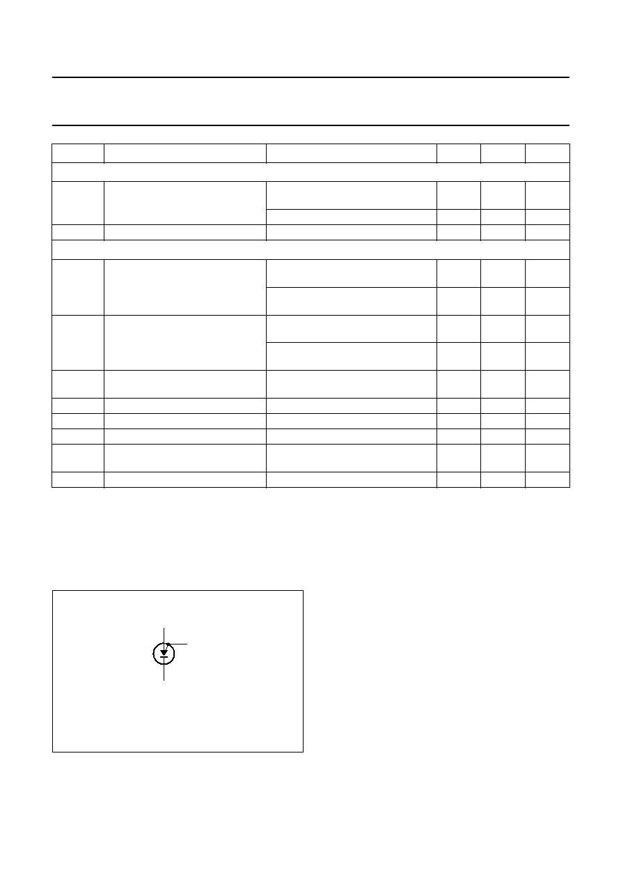
Explanation of symbols
For application of the BRY39 as a programmable
unijunction transistor, only the anode gate is used. To
simplify the symbols, the term gate instead of anode gate
will be used (see Fig.2).
Fig.2
Programmable unijunction transistor
explanation of symbols.
handbook, halfpage
MBB700
g
gate
k
cathode
anode
a