 | –≠–ª–µ–∫—Ç—Ä–æ–Ω–Ω—ã–π –∫–æ–º–ø–æ–Ω–µ–Ω—Ç: BS107 | –°–∫–∞—á–∞—Ç—å:  PDF PDF  ZIP ZIP |
Document Outline
- FEATURES
- DESCRIPTION
- PINNING - TO-92 variant
- QUICK REFERENCE DATA
- LIMITING VALUES
- THERMAL RESISTANCE
- CHARACTERISTICS
- PACKAGE OUTLINE
- DEFINITIONS
- LIFE SUPPORT APPLICATIONS

DATA SHEET
Product specification
File under Discrete Semiconductors, SC13b
April 1995
DISCRETE SEMICONDUCTORS
BS107
N-channel enhancement mode
vertical D-MOS transistor
April 1995
2
Philips Semiconductors
Product specification
N-channel enhancement mode vertical
D-MOS transistor
BS107
FEATURES
∑
Direct interface to C-MOS, TTL,
etc.
∑
High-speed switching
∑
No secondary breakdown.
DESCRIPTION
N-channel enhancement mode
vertical D-MOS transistor in a TO-92
variant envelope. Intended for use as
a line current interruptor in telephone
sets and for applications in relay,
high-speed and line transformer
drivers.
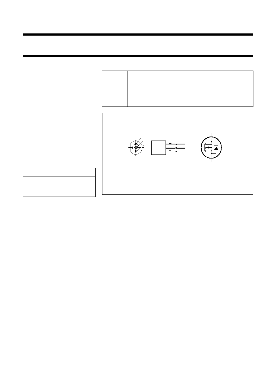
PINNING - TO-92 variant
PIN
DESCRIPTION
1
source
2
gate
3
drain
QUICK REFERENCE DATA
SYMBOL
PARAMETER
MAX.
UNIT
V
DS
drain-source voltage (DC)
200
V
V
GSth
gate-source threshold voltage
2.4
V
I
D
drain current (DC)
150
mA
R
DSon
drain-source on-state resistance
28
Fig.1 Simplified outline and symbol.
handbook, halfpage
1
3
2
MAM146
s
d
g
April 1995
3
Philips Semiconductors
Product specification
N-channel enhancement mode vertical
D-MOS transistor
BS107
LIMITING VALUES
In accordance with the Absolute Maximum System (IEC 134).
THERMAL RESISTANCE
SYMBOL
PARAMETER
CONDITIONS
MIN.
MAX.
UNIT
V
DS
drain-source voltage
-
200
V
±
V
GSO
gate-source voltage
open drain
-
20
V
I
D
drain current
DC
-
150
mA
I
DM
drain current
peak
-
300
mA
P
tot
total power dissipation
up to T
amb
= 25
∞
C
-
830
mW
T
stg
storage temperature range
-
65
150
∞
C
T
j
operating junction temperature
-
150
∞
C
SYMBOL
PARAMETER
MAX.
UNIT
R
th j-a
from junction to ambient
150
K/W

April 1995
4
Philips Semiconductors
Product specification
N-channel enhancement mode vertical
D-MOS transistor
BS107
CHARACTERISTICS
T
j
= 25
∞
C unless otherwise specified.
SYMBOL
PARAMETER
CONDITIONS
MIN.
TYP.
MAX.
UNIT
V
(BR)DSS
drain-source breakdown
voltage
V
GS
= 0
I
D
= 10
µ
A
200
-
-
V
I
DSS
drain-source leakage current
V
DS
= 130 V
V
GS
= 0
-
-
30
nA
I
DSX
drain-source leakage current
V
DS
= 70 V
V
GS
= 0.2 V
-
-
1
µ
A
±
I
GSS
gate-source leakage current
±
V
GS
= 15 V
V
DS
= 0
-
-
10
nA
V
GS(th)
gate threshold voltage
I
D
= 1 mA
V
DS
= V
GS
0.8
-
2.4
V
R
DS(on)
drain-source on-resistance
I
D
= 20 mA
V
GS
= 2.6 V
-
20
28
R
DS(on)
drain-source on-resistance
I
D
= 150 mA
V
GS
= 10 V
-
14
-
Y
fs
transfer admittance
I
D
= 250 mA
V
DS
= 15 V
90
180
-
mS
C
iss
input capacitance
V
DS
= 10 V
V
GS
= 0
f = 1 MHz
-
50
65
pF
C
oss
output capacitance
V
DS
= 10 V
V
GS
= 0
f = 1 MHz
-
16
25
pF
C
rss
feedback capacitance
V
DS
= 10 V
V
GS
= 0
f = 1 MHz
-
4
10
pF
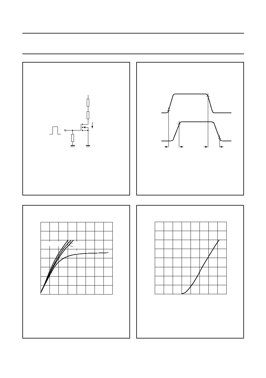
Switching times (see Figs 2 and 3)
t
on
switching-on time
I
D
= 250 mA
V
DD
= 50 V
V
GS
= 0 to 10 V
-
2
10
ns
t
off
switching-off time
I
D
= 250 mA
V
DD
= 50 V
V
GS
= 0 to 10 V
-
4
20
ns
April 1995
5
Philips Semiconductors
Product specification
N-channel enhancement mode vertical
D-MOS transistor
BS107
Fig.2 Switching time test circuit.
handbook, halfpage
MSA631
50
VDD = 50 V
ID
10 V
0 V
Fig.3 Input and output waveforms.
handbook, halfpage
MBB692
10 %
90 %
90 %
10 %
ton
toff
OUTPUT
INPUT
Fig.4 Typical output characteristics; T
j
= 25
∞
C.
handbook, halfpage
0
4
8
VDS (V)
ID
(mA)
16
400
300
100
0
200
12
MDA700
VGS = 10 V
5 V
4 V
3 V
Fig.5
Typical transfer characteristic; V
DS
= 10 V;
T
j
= 25
∞
C.
handbook, halfpage
0
1
2
VGS (V)
ID
(mA)
4
400
300
100
0
200
3
MDA701