 | ÐлекÑÑоннÑй компоненÑ: BS107AMO | СкаÑаÑÑ:  PDF PDF  ZIP ZIP |
N-channel enhancement mode vertical D-MOS transistor

DATA SHEET
Product specification
File under Discrete Semiconductors, SC13b
April 1995
DISCRETE SEMICONDUCTORS
BS107A
N-channel enhancement mode
vertical D-MOS transistor
April 1995
2
Philips Semiconductors
Product specification
N-channel enhancement mode vertical
D-MOS transistor
BS107A
FEATURES
·
Direct interface to C-MOS, TTL,
etc.
·
High-speed switching
·
No second breakdown
DESCRIPTION
N-channel enhancement mode
vertical D-MOS transistor in TO-92
envelope and designed for use as line
current interrupter in telephone sets
and for application in relay,
high-speed and line-transformer
drivers.
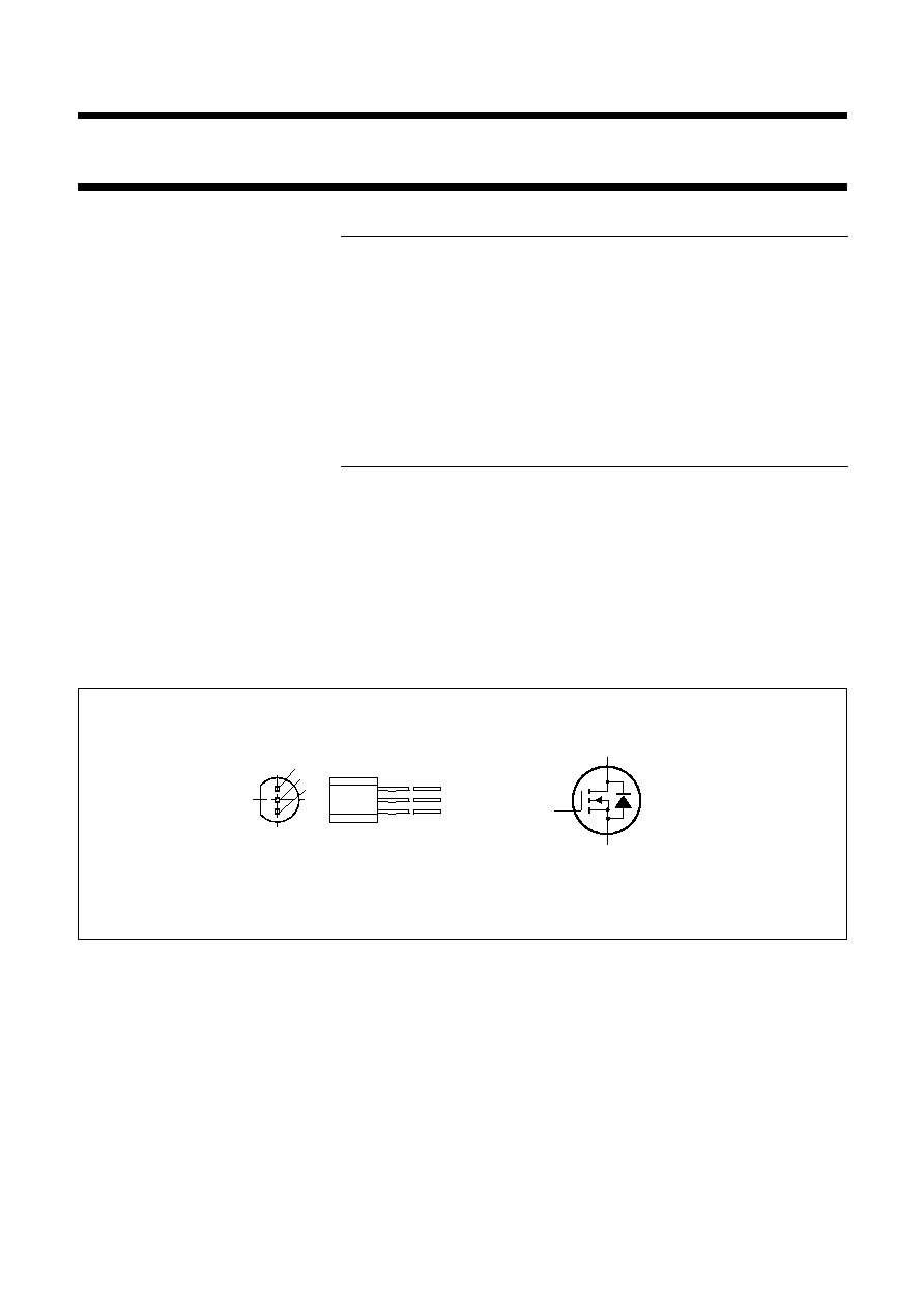
PINNING - TO-92
1
=
source
2
=
gate
3
=
drain
QUICK REFERENCE DATA
Drain-source voltage
V
DS
max.
200 V
Gate-source voltage (open drain)
±
V
GSO
max.
20 V
Drain current (DC)
I
D
max.
250 mA
Total power dissipation up to T
case
= 25
°
C
P
tot
max.
0.6 W
Drain-source ON-resistance
typ.
max.
4.5
6.4
I
D
= 250 mA; V
GS
= 10 V
R
DS(on)
Transfer admittance
min.
typ.
200
350
mS
mS
I
D
= 250 mA; V
GS
= 25 V
Y
fs
PIN CONFIGURATION
Fig.1 Simplified outline and symbol.
Note: Various pinnings are available.
handbook, halfpage
1
3
2
MSB033
handbook, 2 columns
s
d
g
MBB076 - 1

April 1995
3
Philips Semiconductors
Product specification
N-channel enhancement mode vertical
D-MOS transistor
BS107A
RATINGS
Limiting values in accordance with the Absolute Maximum System (IEC 134)
THERMAL RESISTANCE
Note
1. Transistor mounted on printed circuit board, max. lead length 4 mm, mounting pad for collector lead
min. 10 mm
×
10 mm.
Drain-source voltage
V
DS
max.
200 V
Gate-source voltage (open drain)
±
V
GSO
max.
20 V
Drain current (DC)
I
D
max.
250 mA
Drain current (peak)
I
DM
max.
500 mA
Total power dissipation up to T
case
= 25
°
C
P
tot
max.
0.6 W
Storage temperature
T
stg
-
55 to +150
°
C
Junction temperature
T
j
max.
150
°
C
From junction to ambient (note 1)
R
th j-a
=
125 K/W

April 1995
4
Philips Semiconductors
Product specification
N-channel enhancement mode vertical
D-MOS transistor
BS107A
CHARACTERISTICS
T
j
= 25
°
C unless otherwise specified
Drain-source breakdown voltage
I
D
= 10
µ
A; V
GS
= 0
V
(BR)DSS
min.
200 V
Drain-source leakage current
V
DS
= 130 V; V
GS
= 0
I
DSS
max.
30 nA
Gate-source leakage current
V
GS
= 15 V; V
DS
= 0
I
GSS
max.
10 nA
Gate threshold voltage
min.
max.
1.0
3.0
V
V
I
D
= 1 mA; V
DS
= V
GS
V
GS(th)
Drain-source ON-resistance
typ.
max.
4.5
6.4
I
D
= 250 mA; V
GS
= 10 V
R
DSon
I
D
= 100 mA; V
GS
= 10 V
R
DSon
typ.
max.
4.2
6.0
Transfer admittance
min.
typ.
200
350
mS
mS
I
D
= 250 mA; V
DS
= 25 V
y
fs
Input capacitance at f = 1 MHz
V
DS
= 25 V; V
GS
= 0
C
iss
typ.
45 pF
Output capacitance at f = 1 MHz
V
DS
= 25 V; V
GS
= 0
C
oss
typ.
15 pF
Feedback capacitance at f = 1 MHz
V
DS
= 25 V; V
GS
= 0
C
rss
typ.
3.5 pF
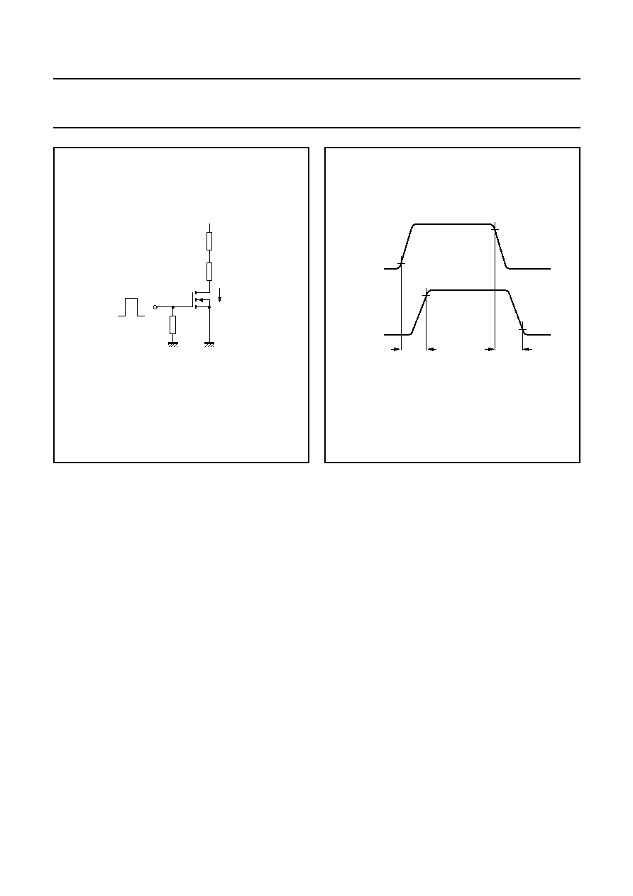
Switching times (see Figs 2 and 3)
I
D
= 250 mA; V
DD
= 50 V; V
GS
= 0 to 10 V
t
on
t
off
typ.
typ.
5
15
ns
ns
April 1995
5
Philips Semiconductors
Product specification
N-channel enhancement mode vertical
D-MOS transistor
BS107A
Fig.2 Switching times test circuit.
handbook, halfpage
MSA631
50
VDD = 50 V
ID
10 V
0 V
Fig.3 Input and output waveforms.
handbook, halfpage
MBB692
10 %
90 %
90 %
10 %
ton
toff
OUTPUT
INPUT
Document Outline
- FEATURES
- DESCRIPTION
- PINNING - TO-92
- QUICK REFERENCE DATA
- PIN CONFIGURATION
- RATINGS
- THERMAL RESISTANCE
- CHARACTERISTICS
- PACKAGE OUTLINE
- DEFINITIONS
- LIFE SUPPORT APPLICATIONS