
Philips Semiconductors
Product specification
Silicon Diffused Power Transistor
BUT11AX
GENERAL DESCRIPTION
High-voltage, high-speed glass-passivated npn power transistor in a plastic full-pack envelope intended for use in
converters, inverters, switching regulators, motor control systems, etc.
QUICK REFERENCE DATA
SYMBOL
PARAMETER
CONDITIONS
TYP.
MAX.
UNIT
V
CESM
Collector-emitter voltage peak value
V
BE
= 0 V
-
1000
V
V
CEO
Collector-emitter voltage (open base)
-
450
V
I
C
Collector current (DC)
-
5
A
I
CM
Collector current peak value
-
10
A
P
tot
Total power dissipation
T
hs
25 �C
-
32
W
V
CEsat
Collector-emitter saturation voltage
-
1.5
V
I
Csat
Collector saturation current
2.5
-
A
t
f
Fall time
150
-
ns
PINNING - SOT186A
PIN CONFIGURATION
SYMBOL
PIN
DESCRIPTION
1
base
2
collector
3
emitter
case isolated
LIMITING VALUES
Limiting values in accordance with the Absolute Maximum Rating System (IEC 134)
SYMBOL
PARAMETER
CONDITIONS
MIN.
MAX.
UNIT
V
CESM
Collector-emitter voltage peak value
V
BE
= 0 V
-
1000
V
V
CEO
Collector-emitter voltage (open base)
-
450
V
I
C
Collector current (DC)
-
5
A
I
CM
Collector current peak value
-
10
A
I
B
Base current (DC)
-
2
A
I
BM
Base current peak value
-
4
A
P
tot
Total power dissipation
T
hs
25 �C
-
32
W
T
stg
Storage temperature
-65
150
�C
T
j
Junction temperature
-
150
�C
THERMAL RESISTANCES
SYMBOL
PARAMETER
CONDITIONS
TYP.
MAX.
UNIT
R
th j-hs
Junction to heatsink
with heatsink compound
-
3.95
K/W
R
th j-a
Junction to ambient
in free air
55
-
K/W
1 2 3
case
b
c
e
November 1995
1
Rev 1.100

Philips Semiconductors
Product specification
Silicon Diffused Power Transistor
BUT11AX
ISOLATION LIMITING VALUE & CHARACTERISTIC
T
hs
= 25 �C unless otherwise specified
SYMBOL
PARAMETER
CONDITIONS
MIN.
TYP.
MAX.
UNIT
V
isol
R.M.S. isolation voltage from all
f = 50-60 Hz; sinusoidal
-
2500
V
three terminals to external
waveform;
heatsink
R.H.
65% ; clean and dustfree
C
isol
Capacitance from T2 to external f = 1 MHz
-
10
-
pF
heatsink
STATIC CHARACTERISTICS
T
hs
= 25 �C unless otherwise specified
SYMBOL
PARAMETER
CONDITIONS
MIN.
TYP.
MAX.
UNIT
I
CES
Collector cut-off current
1
V
BE
= 0 V; V
CE
= V
CESMmax
-
-
1.0
mA
I
CES
V
BE
= 0 V; V
CE
= V
CESMmax
;
-
-
2.0
mA
T
j
= 125 �C
I
EBO
Emitter cut-off current
V
EB
= 9 V; I
C
= 0 A
-
-
10
mA
V
CEOsust
Collector-emitter sustaining voltage
I
B
= 0 A; I
C
= 100 mA;
450
-
-
V
L = 25 mH
V
CEsat
Collector-emitter saturation voltages I
C
= 2.5 A; I
B
= 0.5 A
-
-
1.5
V
V
BEsat
Base-emitter saturation voltage
I
C
= 2.5 A; I
B
= 0.5 A
-
-
1.3
V
h
FE
DC current gain
I
C
= 5 mA; V
CE
= 5 V
10
18
35
h
FE
I
C
= 500 mA; V
CE
= 5 V
10
20
35
DYNAMIC CHARACTERISTICS
T
hs
= 25 �C unless otherwise specified
SYMBOL
PARAMETER
CONDITIONS
TYP.
MAX.
UNIT
Switching times (resistive load)
I
Con
= 2.5 A; I
Bon
= -I
Boff
= 0.5 A
t
on
Turn-on time
0.6
-
�
s
t
s
Turn-off storage time
3.5
-
�
s
t
f
Turn-off fall time
0.6
-
�
s
Switching times (inductive load)
I
Con
= 2.5 A; I
Bon
= 0.5 A; L
B
= 1
�
H;
-V
BB
= 5 V
t
s
Turn-off storage time
1.5
-
�
s
t
f
Turn-off fall time
150
-
ns
Switching times (inductive load)
I
Con
= 2.5 A; I
Bon
= 0.5 A; L
B
= 1
�
H;
-V
BB
= 5 V; T
j
= 100 �C
t
s
Turn-off storage time
1.8
-
�
s
t
f
Turn-off fall time
170
-
ns
1 Measured with half sine-wave voltage (curve tracer).
November 1995
2
Rev 1.100
Philips Semiconductors
Product specification
Silicon Diffused Power Transistor
BUT11AX
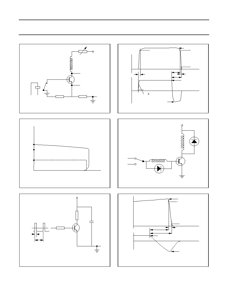
Fig.1. Test circuit for V
CEOsust
.
Fig.2. Oscilloscope display for V
CEOsust
.
Fig.3. Test circuit resistive load. V
IM
= -6 to +8 V
V
CC
= 250 V; t
p
= 20
�
s;
= t
p
/ T = 0.01.
R
B
and R
L
calculated from I
Con
and I
Bon
requirements.
Fig.4. Switching times waveforms with resistive load.
Fig.5. Test circuit inductive load.
V
CC
= 300 V; -V
BE
= 5 V; L
C
= 200 uH; L
B
= 1 uH
Fig.6. Switching times waveforms with inductive load.
+ 50v
100-200R
Horizontal
Vertical
Oscilloscope
1R
6V
30-60 Hz
300R
IC
IB
10 %
10 %
90 %
90 %
ton
toff
ts
tf
IBon
-IBoff
ICon
tr
30ns
VCE / V
min
VCEOsust
IC / mA
100
200
250
0
LB
IBon
-VBB
LC
T.U.T.
VCC
tp
T
VCC
R
R
T.U.T.
0
VIM
B
L
IC
IB
ICon
IBon
-IBoff
t
t
ts
tf
toff
10 %
90 %
November 1995
3
Rev 1.100
Philips Semiconductors
Product specification
Silicon Diffused Power Transistor
BUT11AX
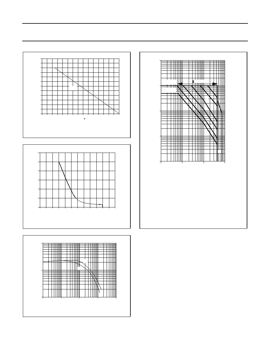
Fig.7. Normalised power derating and second
breakdown curves.
Fig.8. Reverse bias safe operating area. T
j
T
j max
Fig.9. Typical DC current gain.
h
FE
= f(I
C
); parameter V
CE
Fig.10. Forward bias safe operating area. T
hs
25 �C
(1)
P
tot
max and P
tot
peak max lines.
(2)
Second breakdown limits.
I
Region of permissible DC operation.
II
Extension for repetitive pulse operation.
III
Extension during turn-on in single
transistor converters provided that
R
BE
100
and t
p
0.6
�
s.
NB:
Mounted with heatsink compound and
30
�
5 newton force on the centre of the
envelope.
0
20
40
60
80
100
120
140
Ths / C
%
Normalised Derating
120
110
100
90
80
70
60
50
40
30
20
10
0
with heatsink compound
P tot
1
10
100
1000
100
10
1
0.1
0.01
tp =
10 us
100 us
1 ms
10 ms
DC
IC / A
V / V
ICM max
IC max
II
I
= 0.01
III
500 ms
(1)
(2)
CE
6
5
4
3
2
1
0
0
400
800
1200
IC / A
BUT11AX
VCE / V
0.01
0.1
1
10
100
IC / A
h
BUT11AX
100
10
1
FE
1V
5V
November 1995
4
Rev 1.100
Philips Semiconductors
Product specification
Silicon Diffused Power Transistor
BUT11AX
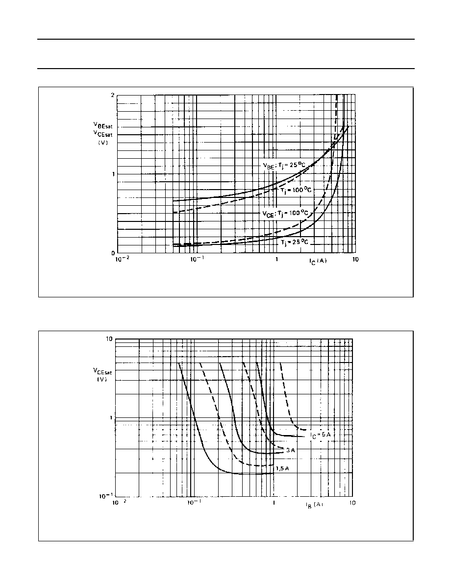
Fig.11. Typical base-emitter and collector-emitter saturation voltages.
V
BEsat
= f(I
C
); V
CEsat
= f(I
C
); I
C
/I
B
= 5
Fig.12. Collector-emitter saturation voltage. Solid lines = typ values,
dotted lines = max values. V
CEsat
= f(I
B
); parameter I
C
November 1995
5
Rev 1.100