 | –≠–ª–µ–∫—Ç—Ä–æ–Ω–Ω—ã–π –∫–æ–º–ø–æ–Ω–µ–Ω—Ç: BZD27-C15 | –°–∫–∞—á–∞—Ç—å:  PDF PDF  ZIP ZIP |
DATA SHEET
Product specification
Supersedes data of October 1991
1996 Jun 10
DISCRETE SEMICONDUCTORS
BZD27 series
Voltage regulator diodes
ok, halfpage
M3D121
1996 Jun 10
2
Philips Semiconductors
Product specification
Voltage regulator diodes
BZD27 series
FEATURES
∑
Glass passivated
∑
High maximum operating
temperature
∑
Low leakage current
∑
Excellent stability
∑
Zener working voltage range:
3.6 to 270 V for 46 types
∑
Transient suppressor stand-off
voltage range: 6.2 to 430 V
for 45 types
∑
Supplied in 8 mm embossed tape.
DESCRIPTION
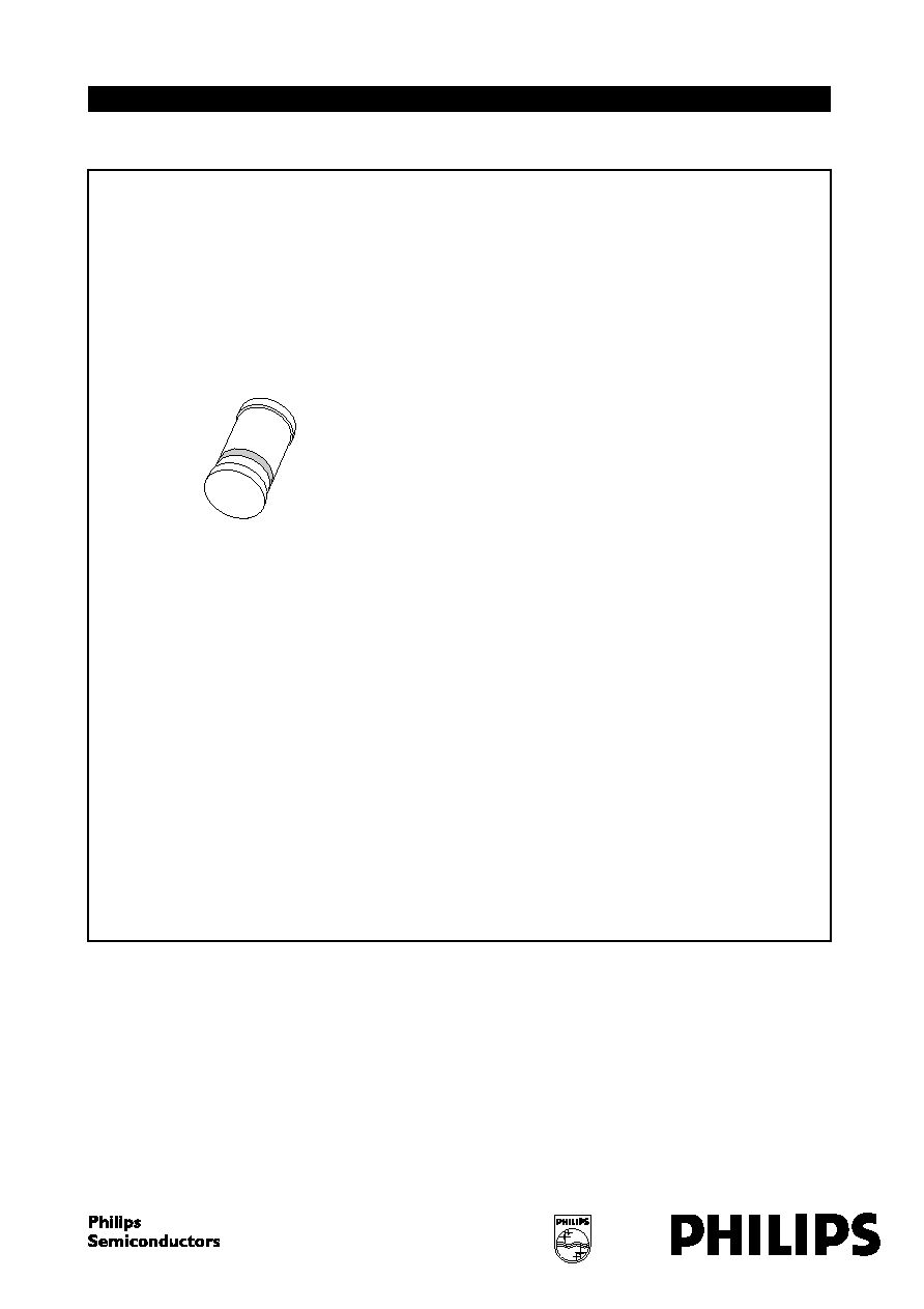
Cavity free cylindrical glass SOD87
package through Implotec
TM
(1)
technology. This package is
hermetically sealed and fatigue free
as coefficients of expansion of all
used parts are matched.
(1) Implotec is a trademark of Philips.
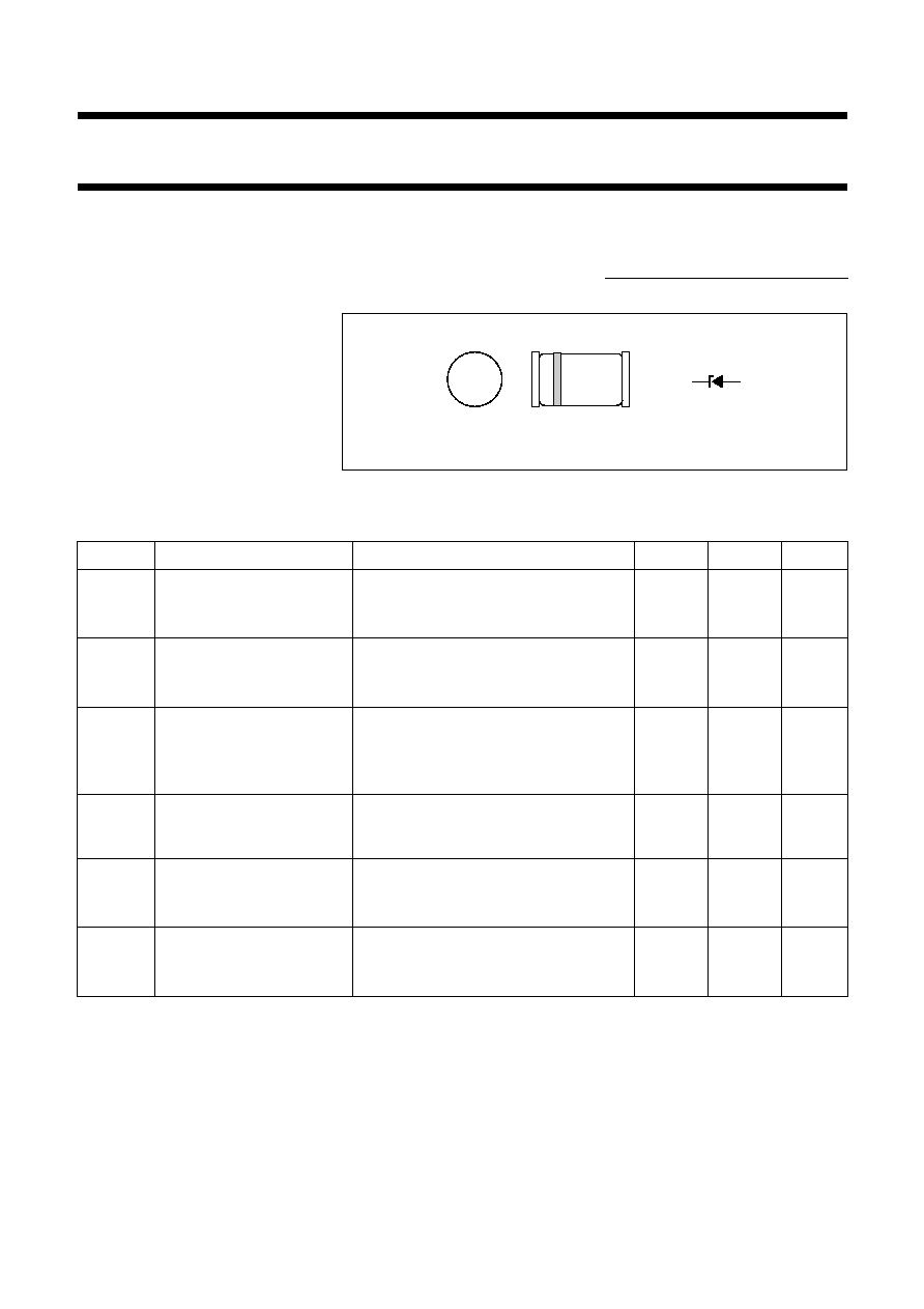
Fig.1 Simplified outline (SOD87) and symbol.
handbook, 4 columns
MAM249
k
a
LIMITING VALUES
In accordance with the Absolute Maximum Rating System (IEC 134).
SYMBOL
PARAMETER
CONDITIONS
MIN.
MAX.
UNIT
P
tot
total power dissipation
T
tp
= 105
∞
C; see Figs 2 and 3
BZD27-C3V6 to -C6V8
-
1.7
W
BZD27-C7V5 to -C510
-
2.3
W
P
tot
total power dissipation
PCB mounted (see Fig.7)
BZD27-C3V6 to -C6V8
T
amb
= 60
∞
C; see Fig.2
-
0.8
W
BZD27-C7V5 to -C510
T
amb
= 55
∞
C; see Fig.3
-
0.8
W
P
ZSM
non-repetitive peak reverse
power dissipation
t
p
= 100
µ
s; square pulse;
T
j
= 25
∞
C prior to surge; see Figs.4 and 5
BZD27-C3V6 to -C6V8
-
300
W
BZD27-C7V5 to -C510
-
300
W
P
RSM
non-repetitive peak reverse
power dissipation
10/1000
µ
s exponential pulse (see Fig.8);
T
j
= 25
∞
C prior to surge
BZD27-C7V5 to -C510
-
150
W
T
stg
storage temperature
BZD27-C3V6 to -C6V8
-
65
+200
∞
C
BZD27-C7V5 to -C510
-
65
+175
∞
C
T
j
junction temperature
BZD27-C3V6 to -C6V8
-
65
+200
∞
C
BZD27-C7V5 to -C510
-
65
+175
∞
C
1996 Jun 10
3
Philips Semiconductors
Product specification
Voltage regulator diodes
BZD27 series
ELECTRICAL CHARACTERISTICS
Total series
T
j
= 25
∞
C unless otherwise specified.
Per type when used as voltage regulator diodes
T
j
= 25
∞
C unless otherwise specified.
SYMBOL
PARAMETER
CONDITIONS
MIN.
MAX.
UNIT
V
F
forward voltage
I
F
= 0.2 A; see Fig.6
-
1.2
V
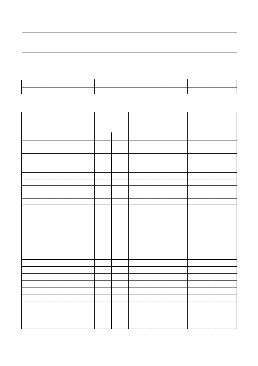
TYPE
No.
SUFFIX
(1)
WORKING VOLTAGE
DIFFERENTIAL
RESISTANCE
TEMPERATURE
COEFFICIENT
TEST
CURRENT
REVERSE CURRENT
at REVERSE VOLTAGE
V
Z
(V) at I
Z
r
dif
(
) at I
Z
S
Z
(%/K) at I
Z
I
Z
(mA)
I
R
(
µ
A)
V
R
(V)
MIN.
NOM.
MAX.
TYP.
MAX.
MIN.
MAX.
MAX.
C3V6
3.4
3.6
3.8
4
8
-
0.14
-
0.04
100
100
1
C3V9
3.7
3.9
4.1
4
8
-
0.14
-
0.04
100
50
1
C4V3
4.0
4.3
4.6
4
7
-
0.12
-
0.02
100
25
1
C4V7
4.4
4.7
5.0
3
7
-
0.10
0.00
100
10
1
C5V1
4.8
5.1
5.4
3
6
-
0.08
-
0.02
100
5
1
C5V6
5.2
5.6
6.0
2
4
-
0.04
0.04
100
10
2
C6V2
5.8
6.2
6.6
2
3
-
0.01
0.06
100
5
2
C6V8
6.4
6.8
7.2
1
3
0.00
0.07
100
10
3
C7V5
7.0
7.5
7.9
1
2
0.00
0.07
100
50
3
C8V2
7.7
8.2
8.7
1
2
0.03
0.08
100
10
3
C9V1
8.5
9.1
9.6
2
4
0.03
0.08
50
10
5
C10
9.4
10
10.6
2
4
0.05
0.09
50
7
7.5
C11
10.4
11
11.6
4
7
0.05
0.10
50
4
8.2
C12
11.4
12
12.7
4
7
0.05
0.10
50
3
9.1
C13
12.4
13
14.1
5
10
0.05
0.10
50
2
10
C15
13.8
15
15.6
5
10
0.05
0.10
50
1
11
C16
15.3
16
17.1
6
15
0.06
0.11
25
1
12
C18
16.8
18
19.1
6
15
0.06
0.11
25
1
13
C20
18.8
20
21.2
6
15
0.06
0.11
25
1
15
C22
20.8
22
23.3
6
15
0.06
0.11
25
1
16
C24
22.8
24
25.6
7
15
0.06
0.11
25
1
18
C27
25.1
27
28.9
7
15
0.06
0.11
25
1
20
C30
28
30
32
8
15
0.06
0.11
25
1
22
C33
31
33
35
8
15
0.06
0.11
25
1
24
C36
34
36
38
21
40
0.06
0.11
10
1
27
C39
37
39
41
21
40
0.06
0.11
10
1
30
C43
40
43
46
24
45
0.07
0.12
10
1
33
C47
44
47
50
24
45
0.07
0.12
10
1
36

1996 Jun 10
4
Philips Semiconductors
Product specification
Voltage regulator diodes
BZD27 series
Note
1. To complete the type number the suffix is added to the basic type number, e.g. BZD27-C51.
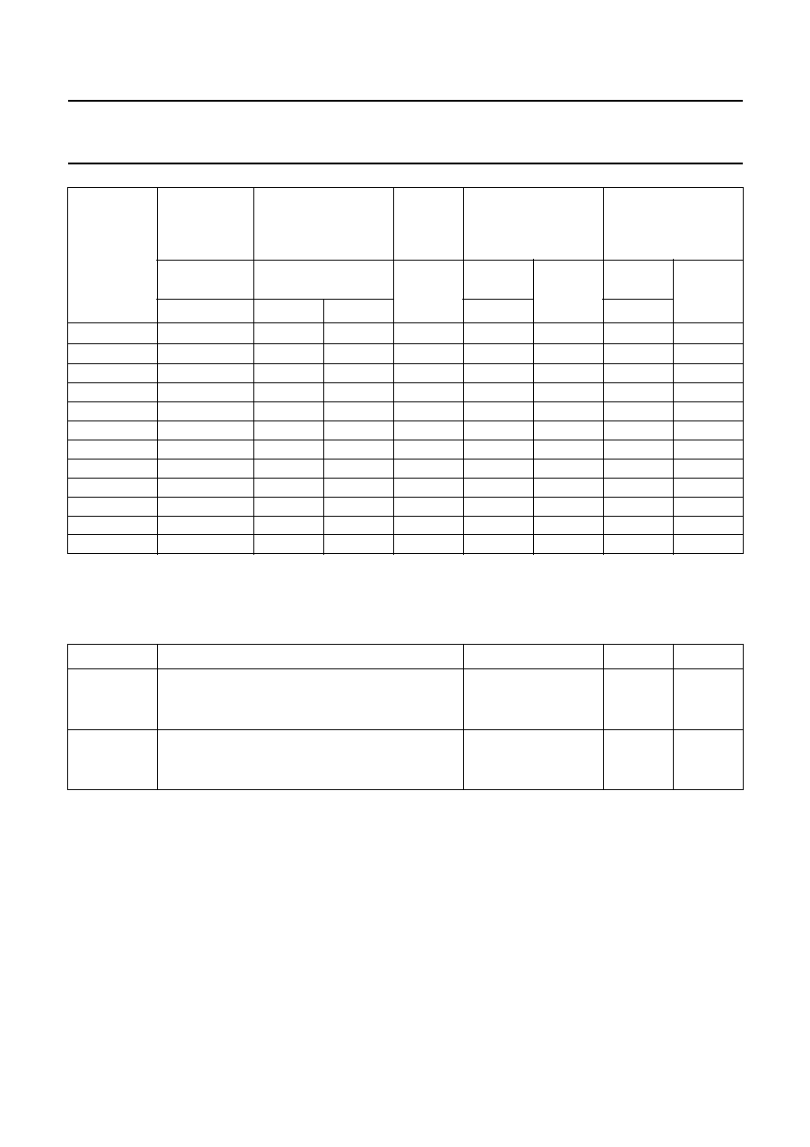
C51
48
51
54
25
60
0.07
0.12
10
1
39
C56
52
56
60
25
60
0.07
0.12
10
1
43
C62
58
62
66
25
80
0.08
0.13
10
1
47
C68
64
68
72
25
80
0.08
0.13
10
1
51
C75
70
75
79
30
100
0.08
0.13
10
1
56
C82
77
82
87
30
100
0.08
0.13
10
1
62
C91
85
91
96
60
200
0.09
0.13
5
1
68
C100
94
100
106
60
200
0.09
0.13
5
1
75
C110
104
110
116
80
250
0.09
0.13
5
1
82
C120
114
120
127
80
250
0.09
0.13
5
1
91
C130
124
130
141
110
300
0.09
0.13
5
1
100
C150
138
150
156
130
300
0.09
0.13
5
1
110
C160
153
160
171
150
350
0.09
0.13
5
1
120
C180
168
180
191
180
400
0.09
0.13
5
1
130
C200
188
200
212
200
500
0.09
0.13
5
1
150
C220
208
220
233
350
750
0.09
0.13
2
1
160
C240
228
240
256
400
850
0.09
0.13
2
1
180
C270
251
270
289
450
1000
0.09
0.13
2
1
200
TYPE
No.
SUFFIX
(1)
WORKING VOLTAGE
DIFFERENTIAL
RESISTANCE
TEMPERATURE
COEFFICIENT
TEST
CURRENT
REVERSE CURRENT
at REVERSE VOLTAGE
V
Z
(V) at I
Z
r
dif
(
) at I
Z
S
Z
(%/K) at I
Z
I
Z
(mA)
I
R
(
µ
A)
V
R
(V)
MIN.
NOM.
MAX.
TYP.
MAX.
MIN.
MAX.
MAX.

1996 Jun 10
5
Philips Semiconductors
Product specification
Voltage regulator diodes
BZD27 series
Per type when used as transient suppressor diodes
T
j
= 25
∞
C unless otherwise specified.
TYPE
NUMBER
REVERSE
BREAKDOWN
VOLTAGE
TEMPERATURE
COEFFICIENT
TEST
CURREN
T
CLAMPING
VOLTAGE
REVERSE
CURRENT at
STAND-OFF
VOLTAGE
V
(BR)R
(V)
at I
test
S
Z
(%/K) at I
test
I
test
(mA)
V
(CL)R
(V)
at I
RSM
(A)
note 1
I
R
(
µ
A)
at V
R
(V)
MIN.
MIN.
MAX.
MAX.
MAX.
BZD27-C7V5
7.0
0.00
0.07
100
11.3
13.3
1500
6.2
BZD27-C8V2
7.7
0.03
0.08
100
12.3
12.2
1200
6.8
BZD27-C9V1
8.5
0.03
0.08
50
13.3
11.3
100
7.5
BZD27-C10
9.4
0.05
0.09
50
14.8
10.1
20
8.2
BZD27-C11
10.4
0.05
0.10
50
15.7
9.6
5
9.1
BZD27-C12
11.4
0.05
0.10
50
17.0
8.8
5
10
BZD27-C13
12.4
0.05
0.10
50
18.9
7.9
5
11
BZD27-C15
13.8
0.05
0.10
50
20.9
7.2
5
12
BZD27-C16
15.3
0.06
0.11
25
22.9
6.6
5
13
BZD27-C18
16.8
0.06
0.11
25
25.6
5.9
5
15
BZD27-C20
18.8
0.06
0.11
25
28.4
5.3
5
16
BZD27-C22
20.8
0.06
0.11
25
31.0
4.8
5
18
BZD27-C24
22.8
0.06
0.11
25
33.8
4.4
5
20
BZD27-C27
25.1
0.06
0.11
25
38.1
3.9
5
22
BZD27-C30
28
0.06
0.11
25
42.2
3.6
5
24
BZD27-C33
31
0.06
0.11
25
46.2
3.2
5
27
BZD27-C36
34
0.06
0.11
10
50.1
3.0
5
30
BZD27-C39
37
0.06
0.11
10
54.1
2.8
5
33
BZD27-C43
40
0.07
0.12
10
60.7
2.5
5
36
BZD27-C47
44
0.07
0.12
10
65.5
2.3
5
39
BZD27-C51
48
0.07
0.12
10
70.8
2.1
5
43
BZD27-C56
52
0.07
0.12
10
78.6
1.9
5
47
BZD27-C62
58
0.08
0.13
10
86.5
1.7
5
51
BZD27-C68
64
0.08
0.13
10
94.4
1.6
5
56
BZD27-C75
70
0.08
0.13
10
103.5
1.5
5
62
BZD27-C82
77
0.08
0.13
10
114
1.3
5
68
BZD27-C91
85
0.09
0.13
5
126
1.2
5
75
BZD27-C100
94
0.09
0.13
5
139
1.1
5
82
BZD27-C110
104
0.09
0.13
5
152
1.0
5
91
BZD27-C120
114
0.09
0.13
5
167
0.90
5
100
BZD27-C130
124
0.09
0.13
5
185
0.81
5
110
BZD27-C150
138
0.09
0.13
5
204
0.73
5
120
BZD27-C160
153
0.09
0.13
5
224
0.67
5
130
1996 Jun 10
6
Philips Semiconductors
Product specification
Voltage regulator diodes
BZD27 series
Note
1. Non-repetitive peak reverse current in accordance with
"IEC 60-1, Section 8" (10/1000
µ
s pulse); see Fig.8.
THERMAL CHARACTERISTICS
Note
1. Device mounted on an epoxy-glass printed-circuit board, 1.5 mm thick; thickness of Cu-layer
40
µ
m, see Fig.7.
For more information please refer to the
"General Part of associated Handbook".
BZD27-C180
168
0.09
0.13
5
249
0.60
5
150
BZD27-C200
188
0.09
0.13
5
276
0.54
5
160
BZD27-C220
208
0.09
0.13
2
305
0.50
5
180
BZD27-C240
228
0.09
0.13
2
336
0.45
5
200
BZD27-C270
251
0.09
0.13
2
380
0.40
5
220
BZD27-C300
280
0.09
0.13
2
419
0.36
5
240
BZD27-C330
310
0.09
0.13
2
459
0.33
5
270
BZD27-C360
340
0.09
0.13
2
498
0.30
5
300
BZD27-C390
370
0.09
0.13
2
537
0.28
5
330
BZD27-C430
400
0.09
0.13
2
603
0.25
5
360
BZD27-C470
440
0.09
0.13
2
655
0.23
5
390
BZD27-C510
480
0.09
0.13
2
707
0.21
5
430
SYMBOL
PARAMETER
CONDITIONS
VALUE
UNIT
R
th j-tp
thermal resistance from junction to tie-point
BZD27-C3V6 to -C6V8
55
K/W
BZD27-C7V5 to -C510
30
K/W
R
th j-a
thermal resistance from junction to ambient
note 1
BZD27-C3V6 to -C6V8
175
K/W
BZD27-C7V5 to -C510
150
K/W
TYPE
NUMBER
REVERSE
BREAKDOWN
VOLTAGE
TEMPERATURE
COEFFICIENT
TEST
CURREN
T
CLAMPING
VOLTAGE
REVERSE
CURRENT at
STAND-OFF
VOLTAGE
V
(BR)R
(V)
at I
test
S
Z
(%/K) at I
test
I
test
(mA)
V
(CL)R
(V)
at I
RSM
(A)
note 1
I
R
(
µ
A)
at V
R
(V)
MIN.
MIN.
MAX.
MAX.
MAX.
1996 Jun 10
7
Philips Semiconductors
Product specification
Voltage regulator diodes
BZD27 series
GRAPHICAL DATA
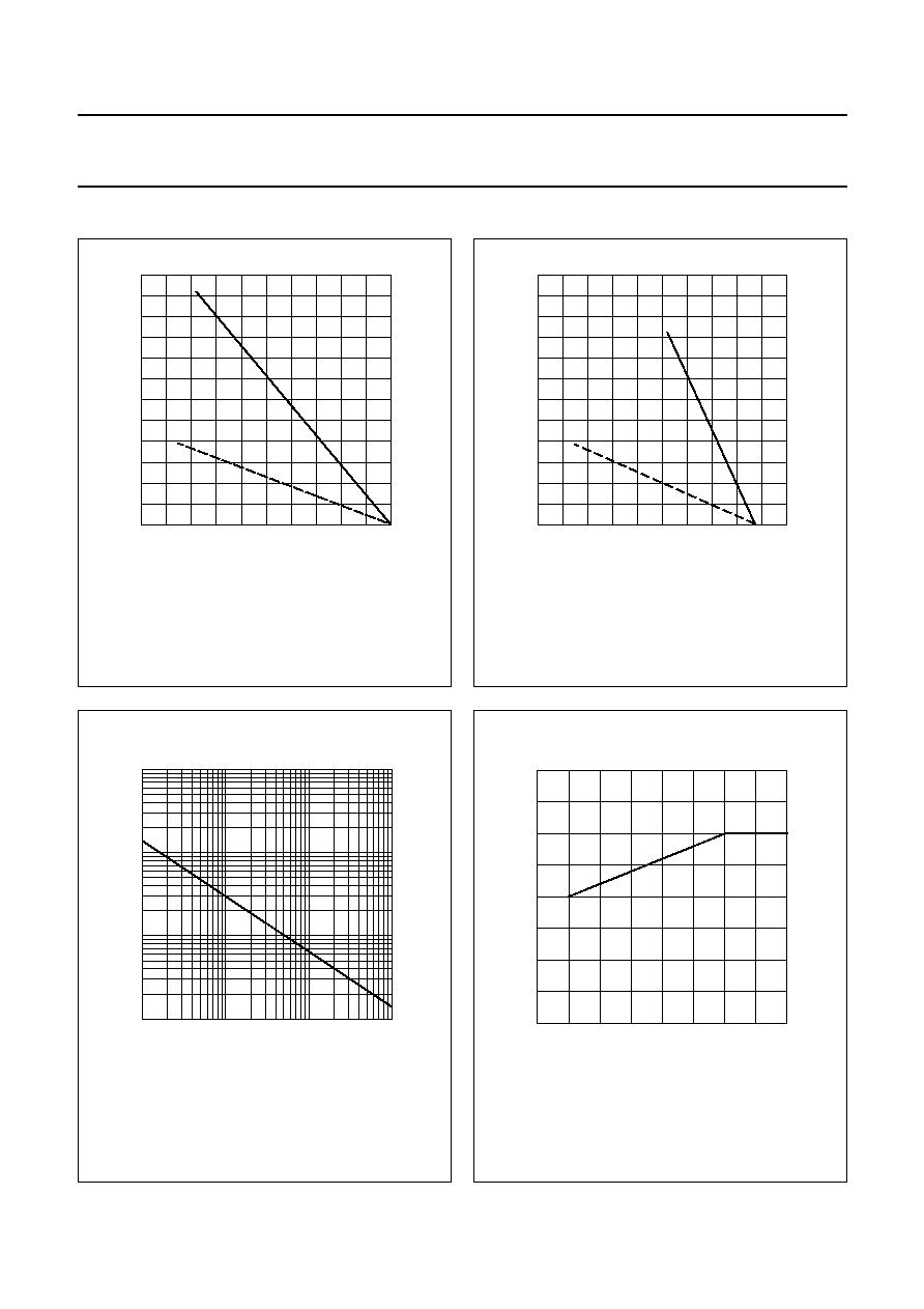
Fig.2
Maximum total power dissipation as a
function of temperature.
Types BZD27-C3V6 to -C6V8
Solid line: tie-point temperature.
Dotted line: ambient temperature;
device mounted as shown in Fig.7.
handbook, halfpage
0
200
3
0
1
2
MBH454
Ptot
(W)
100
T (
∞
C)
Fig.3
Maximum total power dissipation as a
function of temperature.
Types BZD27-C7V5 to -C510
Solid line: tie-point temperature.
Dotted line: ambient temperature;
device mounted as shown in Fig.7.
handbook, halfpage
0
200
3
0
1
2
MBH455
Ptot
(W)
100
T (
∞
C)
T
j
= 25
∞
C prior to surge.
See also Fig 5.
Fig.4
Maximum non-repetitive peak reverse
power dissipation as a function of pulse
duration (square pulse).
handbook, halfpage
10
-
2
10
10
2
10
3
10
4
10
-
1
1
tp (ms)
PZSM
(W)
10
MGD524
T
j
= 25
∞
C prior to surge.
Fig.5
Maximum non-repetitive peak reverse
power dissipation as a function of nominal
working voltage.
handbook, halfpage
0
3V9
4V7
6V8
400
300
100
0
200
MGD525
5V6
VZnom (V)
3V6
4V3
6V2
5V1
PZSM
(W)
1996 Jun 10
8
Philips Semiconductors
Product specification
Voltage regulator diodes
BZD27 series
T
j
= 25
∞
C.
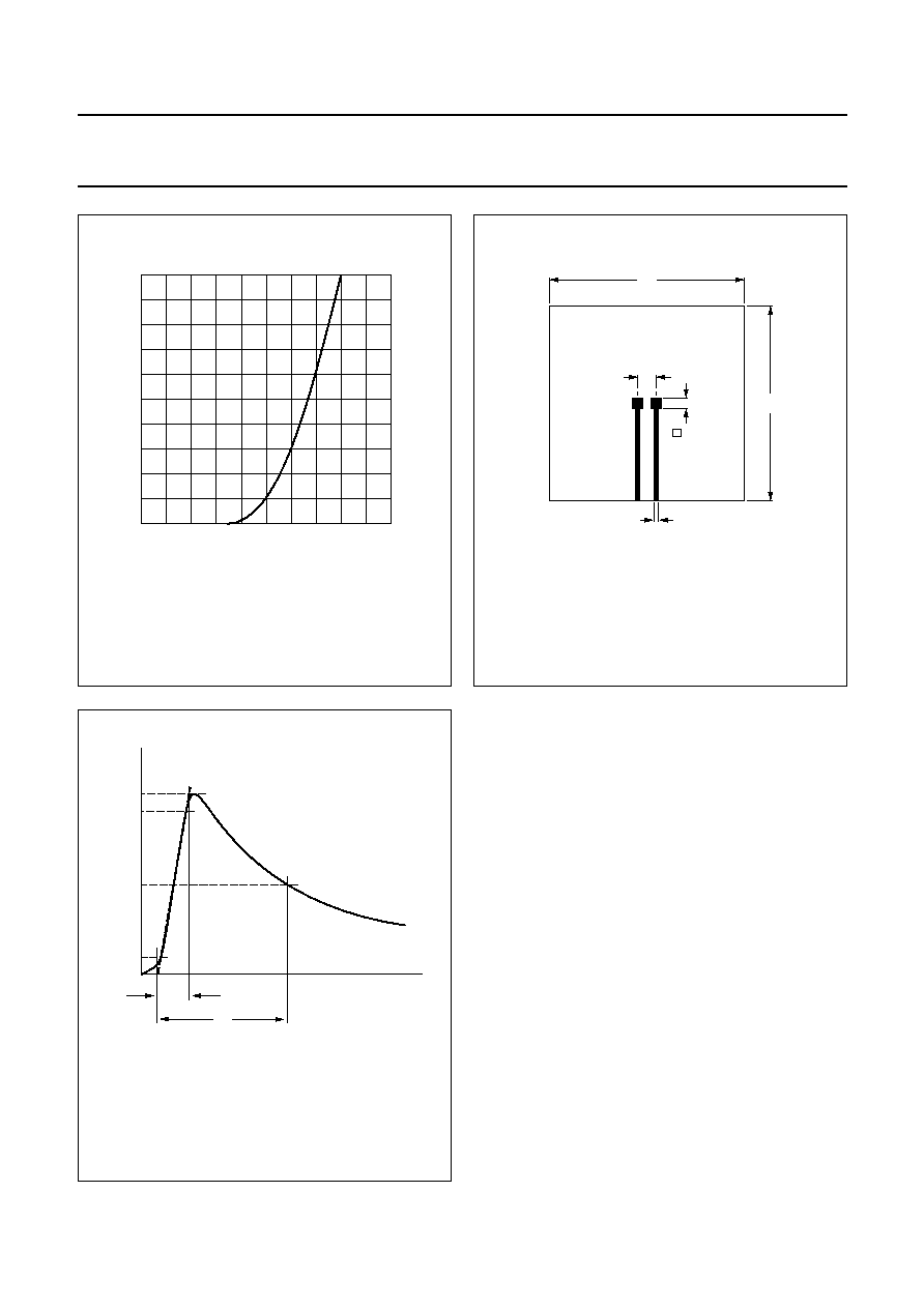
Fig.6
Forward current as a function of forward
voltage; typical values.
handbook, halfpage
0
2
2
IF
(A)
0
MGD520
1
1
VF (V)
Fig.7 Printed-circuit board for surface mounting.
Dimensions in mm.
MSB213
4.5
2.5
1.25
50
50
Fig.8
Non-repetitive peak reverse current
pulse definition.
In accordance with
"IEC 60-1, Section 8".
t
1
= 10
µ
s.
t
2
= 1000
µ
s.
handbook, halfpage
MGD521
IRSM
(%)
100
90
50
10
t1
t2
t
1996 Jun 10
9
Philips Semiconductors
Product specification
Voltage regulator diodes
BZD27 series
PACKAGE OUTLINE
DEFINITIONS
LIFE SUPPORT APPLICATIONS
These products are not designed for use in life support appliances, devices, or systems where malfunction of these
products can reasonably be expected to result in personal injury. Philips customers using or selling these products for
use in such applications do so at their own risk and agree to fully indemnify Philips for any damages resulting from such
improper use or sale.
Data sheet status
Objective specification
This data sheet contains target or goal specifications for product development.
Preliminary specification
This data sheet contains preliminary data; supplementary data may be published later.
Product specification
This data sheet contains final product specifications.
Limiting values
Limiting values given are in accordance with the Absolute Maximum Rating System (IEC 134). Stress above one or
more of the limiting values may cause permanent damage to the device. These are stress ratings only and operation
of the device at these or at any other conditions above those given in the Characteristics sections of the specification
is not implied. Exposure to limiting values for extended periods may affect device reliability.
Application information
Where application information is given, it is advisory and does not form part of the specification.
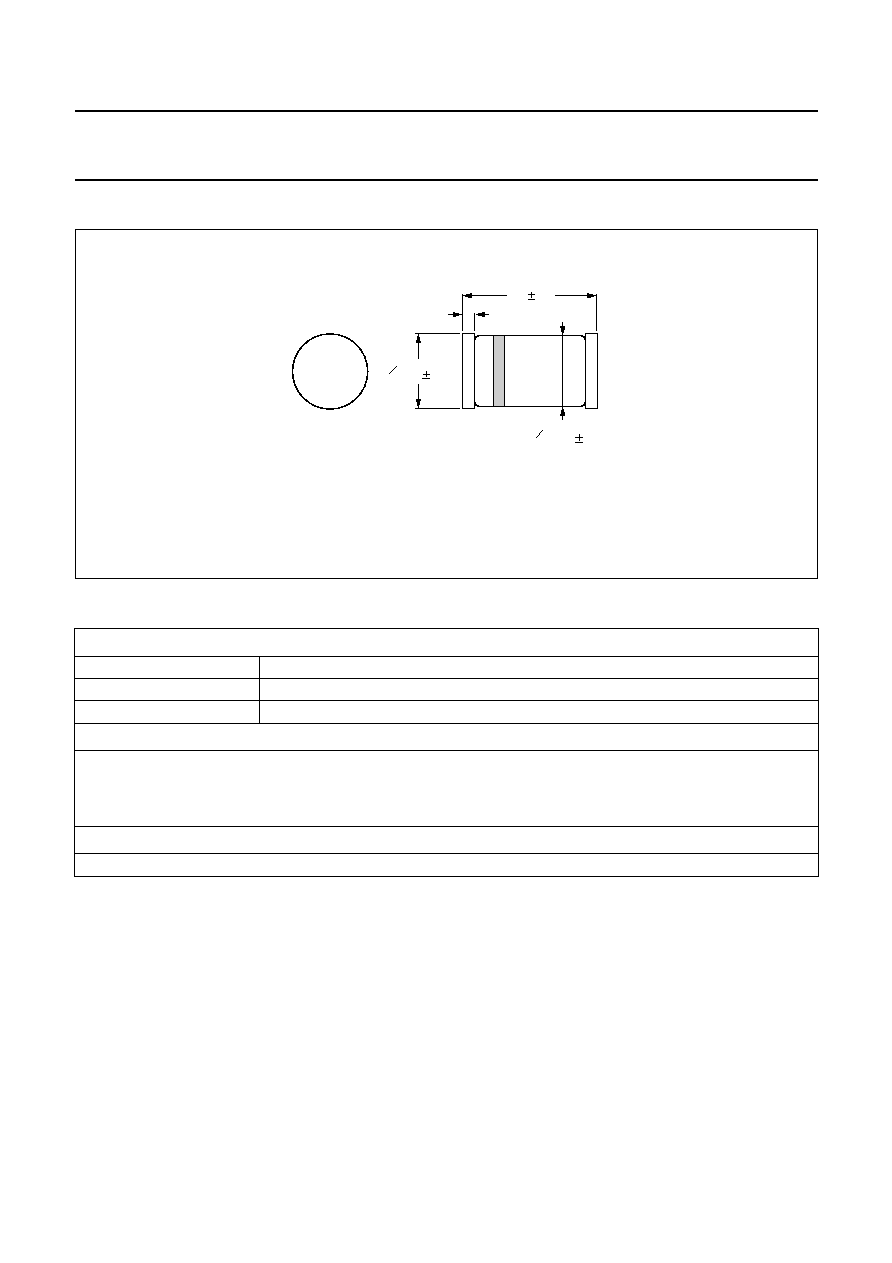
Dimensions in mm.
The marking band indicates the cathode.
Fig.9 SOD87.
handbook, full pagewidth
MBA505
0.3
O
2.05
0.05
D =
3.5 0.2
D1 =
1.9
0.1
O