 | ÐлекÑÑоннÑй компоненÑ: CBT3245A | СкаÑаÑÑ:  PDF PDF  ZIP ZIP |
Äîêóìåíòàöèÿ è îïèñàíèÿ www.docs.chipfind.ru
Philips
Semiconductors
CBT3245A
Octal bus switch
Product data
Supersedes data of 2002 Feb 18
2003 Jun 27
INTEGRATED CIRCUITS
Philips Semiconductors
Product data
CBT3245A
Octal bus switch
2
2003 Jun 27
FEATURES
·
Standard '245-type pinout
·
5
switch connection between two ports
·
TTL compatible control input levels
·
Package options include plastic small outline (D), shrink small
outline (DB), thin shrink small outline (TSSOP)
·
Latch-up protection exceeds 500 mA per JESD78
·
ESD protection exceeds 2000 V HBM per JESD22-A114,
150 V MM per JESD22-A115 and 1000 V CDM per JESD22-C101
DESCRIPTION
The CBT3245A provides eight bits of high-speed TTL-compatible
bus switching in a standard '245 device pinout. The low on-state
resistance of the switch allows connections to be made with minimal
propagation delay.
The CBT3245A device is organized as one 8-bit switch. When
enable (OE) is LOW, the switch is on and port A is connected to
port B. When OE is HIGH, the switch is open and a high-impedance
state exists between the two ports.
The CBT3245A is characterized for operation from -40 to +85
°
C.
PIN CONFIGURATION -- SO, SSOP, QSOP, AND
TSSOP
1
2
3
4
5
6
7
8
9
10
11
12
13
14
15
16
17
18
19
20
NC
A1
A2
A3
A4
A5
A6
A7
A8
B7
GND
B6
B5
B4
B3
B2
B1
OE
VCC
B8
SA00507
Figure 1. Pin configuration -- SO, SSOP, QSOP, and TSSOP
PIN CONFIGURATION -- DHVQFN
2
1
3
4
5
6
7
8
9
10
11
12
13
14
15
16
17
18
19
20
NC
A1
A2
A3
A4
A5
A6
A7
A8
B7
GND
B6
B5
B4
B3
B2
B1
OE
VCC
B8
SA00649
GND*
* THE DIE SUBSTRATE IS ATTACHED TO THIS PAD USING CONDUCTIVE DIE
ATTACH MATERIAL. IT CANNOT BE USED AS A SUPPLY PIN OR INPUT.
** PIN 1 INDICATION DOT
**
Figure 2. Pin configuration -- DHVQFN (top view)
PIN DESCRIPTION
PIN NUMBER
SYMBOL
NAME AND FUNCTION
1
NC
No internal connection
19
OE
Output enable input
2, 3, 4, 5, 6, 7, 8, 9
A1-A8
Inputs
18, 17, 16, 15, 14,
13, 12, 11
B1-B8
Outputs
10
GND
Ground (0V)
20
V
CC
Positive supply voltage
ORDERING INFORMATION
PACKAGES
TEMPERATURE RANGE
ORDER CODE
TOPSIDE MARK
DWG NUMBER
20-Pin Plastic DHVQFN
-40 to 85
°
C
CBT3245ABQ
CT3245A
SOT764-1
20-Pin Plastic TSSOP
-40 to 85
°
C
CBT3245APW
CT3245A
SOT360-1
20-Pin Plastic SSOP (QSOP)
-40 to 85
°
C
CBT3245ADS
CT3245ADS
SOT724-1
20-Pin Plastic SSOP
-40 to 85
°
C
CBT3245ADB
CT3245A
SOT339-1
20-Pin Plastic SO
-40 to 85
°
C
CBT3245AD
CBT3245AD
SOT163-1
Standard packing quantities and other packaging data is available at www.philipslogic.com/packaging.
Philips Semiconductors
Product data
CBT3245A
Octal bus switch
2003 Jun 27
3
LOGIC SYMBOL
SA00508
A1
A8
B1
B8
2
9
18
11
19
OE
FUNCTION TABLE
INPUT
INPUTS/OUTPUTS
OE
A, B
L
A = B
H
Z
H = HIGH voltage level
L
= LOW voltage level
Z = HIGH impedance "off" state
ABSOLUTE MAXIMUM RATINGS
1, 2
SYMBOL
PARAMETER
CONDITIONS
RATING
UNIT
V
CC
DC supply voltage
-0.5 to +7.0
V
I
IK
DC input diode current
V
I
< 0
-50
mA
V
I
DC input voltage
3
-0.5 to +7.0
V
I
OK
DC output diode current
V
O
< 0
-50
mA
V
OUT
DC output voltage
3
output in Off or HIGH state
-0.5 to +7
V
I
OUT
DC output current
output in LOW state
128
mA
T
stg
Storage temperature range
-65 to 150
°
C
NOTES:
1. Stresses beyond those listed may cause permanent damage to the device. These are stress ratings only and functional operation of the
device at these or any other conditions beyond those indicated under "recommended operating conditions" is not implied. Exposure to
absolute-maximum-rated conditions for extended periods may affect device reliability.
2. The performance capability of a high-performance integrated circuit in conjunction with its thermal environment can create junction
temperatures which are detrimental to reliability. The maximum junction temperature of this integrated circuit should not exceed 150
°
C.
3. The input and output voltage ratings may be exceeded if the input and output current ratings are observed.
RECOMMENDED OPERATING CONDITIONS
LIMITS
SYMBOL
PARAMETER
MIN
MAX
UNIT
V
CC
DC supply voltage
4.0
5.5
V
V
IH
HIGH-level input voltage
2.0
--
V
V
IL
LOW-level input voltage
--
0.8
V
T
amb
Operating free-air temperature range
-40
+85
°
C
Philips Semiconductors
Product data
CBT3245A
Octal bus switch
2003 Jun 27
4
DC ELECTRICAL CHARACTERISTICS
LIMITS
SYMBOL
PARAMETER
TEST CONDITIONS
T
amb
= -40 to +85
°
C
UNIT
MIN
TYP
1
MAX
V
IK
Input clamp voltage
V
CC
= 4.5 V; I
I
= -18 mA
--
--
-1.2
V
I
I
Input leakage current
V
CC
= 5.5 V; V
I
= GND or 5.5 V
--
--
±
5
µ
A
I
CC
Quiescent supply current
V
CC
= 5.5 V; I
O
= 0, V
I
= V
CC
or GND
--
1
3
µ
A
I
CC
Additional supply current per
input pin
2
V
CC
= 5.5 V, one input at 3.4 V, other inputs at
V
CC
or GND
--
--
3.5
mA
C
I
Control pins
V
I
= 3 V or 0, OE = V
CC
--
3.2
--
pF
C
IO(OFF)
Pin capacitance (OFF state)
V
O
= 3 V or 0
--
6.6
--
pF
V
CC
= 4.5 V; V
1
= 0 V; I
I
= 64 mA
--
5
7
r
on
3
On-resistance
V
CC
= 4.5 V; V
1
= 0 V; I
I
= 30 mA
--
5
7
V
CC
= 4.5 V; V
1
= 2.4 V; I
I
= 15 mA
--
10
15
NOTES:
1. All typical values are at V
CC
= 5 V, T
amb
= 25
°
C
2. This is the increase in supply current for each input that is at the specified TTL voltage level rather than V
CC
or GND
3. Measured by the voltage drop between the A and the B terminals at the indicated current through the switch.
On-state resistance is determined by the lowest voltage of the two (A or B) terminals.
AC CHARACTERISTICS
GND = 0 V; t
R;
C
L
= 50 pF
CBT3245A
SYMBOL
PARAMETER
FROM
(INPUT)
TO
(OUTPUT)
T
amb
= -40 to +85
°
C
V
CC
= +5.0 V
±
0.5 V
UNIT
MIN
MAX
t
pd
Propagation delay
1
A or B
B or A
--
0.25
ns
t
en
Output enable time
to HIGH and LOW level
OE
A or B
1.0
5.9
ns
t
dis
Output disable time
from HIGH and LOW level
OE
A or B
1.0
6.0
ns
NOTES:
1. This parameter is warranted but not production tested. The propagation delay is based on the RC time constant of the typical on-state
resistance of the switch and a load capacitance of 50 pF, when driven by an ideal voltage source (zero output impedance).
Philips Semiconductors
Product data
CBT3245A
Octal bus switch
2003 Jun 27
5
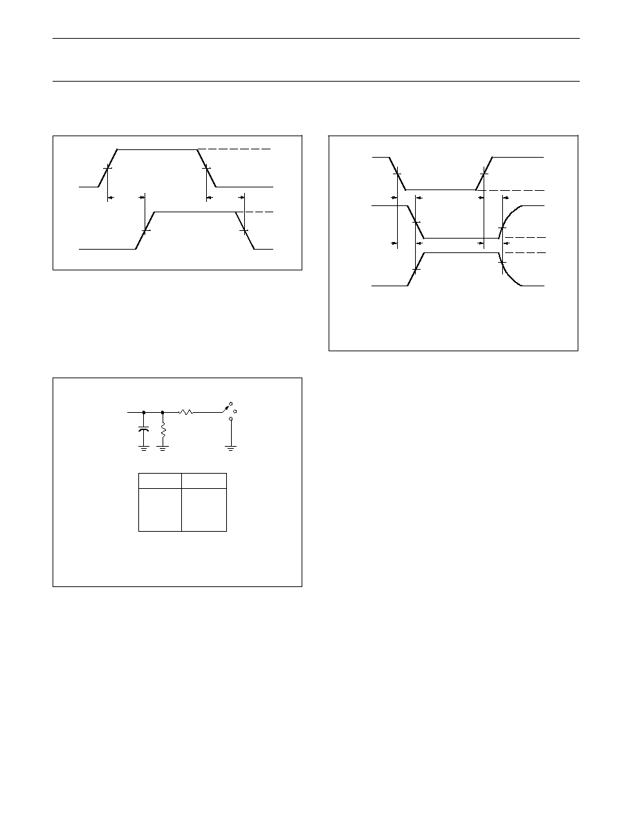
AC WAVEFORMS
V
M
= 1.5 V, V
IN
= GND to 3.0 V
INPUT
1.5 V
OUTPUT
t
PLH
t
PHL
SA00028
1.5 V
1.5 V
1.5 V
3 V
0 V
V
OH
V
OL
Waveform 1. Input to Output Propagation Delays
Output Control
(Low-level
enabling )
1.5 V
t
PZH
t
PHZ
V
OH
V
OL
t
PZL
t
PLZ
3.5 V
0 V
V
OL
+ 0.3 V
V
OH
- 0.3 V
SA00029
1.5 V
1.5 V
1.5 V
0 V
3 V
Output
Waveform 1
S1 at 7 V
(see Note)
Note:
Waveform 1 is for an output with internal conditions such that
the output is low except when disabled by the output control.
Waveform 2 is for an output with internal conditions such that
the output is high except when disabled by the output control.
Output
Waveform 2
S1 at Open
(see Note)
Waveform 2. 3-State Output Enable and Disable Times
TEST CIRCUIT AND WAVEFORMS
C
L
= 50 pF
500
Load Circuit
DEFINITIONS
C
L
=
Load capacitance includes jig and probe capacitance;
see AC CHARACTERISTICS for value.
TEST
S1
t
pd
open
t
PLZ
/t
PZL
7 V
t
PHZ
/t
PZH
open
SA00012
500
From Output
Under Test
S1
7 V
Open
GND
NOTES:
1. All input pulses are supplied by generators having the following characteristics: PRR
10 MHz, Z
O
= 50
, t
r
2.5 ns, t
f
2.5 ns.
2. The outputs are measured one at a time with one transition per measurement.
Philips Semiconductors
Product data
CBT3245A
Octal bus switch
2003 Jun 27
6
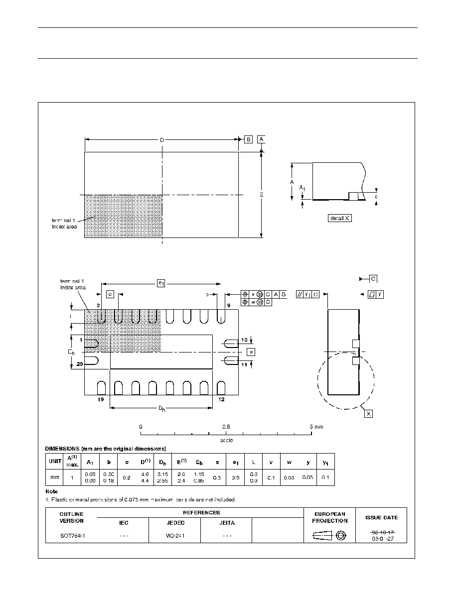
DHVQFN20:
plastic dual in-line compatible thermal enhanced very thin quad flat package;
no leads; 20 terminals; body 2.5 x 4.5 x 0.85 mm
SOT764-1
Philips Semiconductors
Product data
CBT3245A
Octal bus switch
2003 Jun 27
7
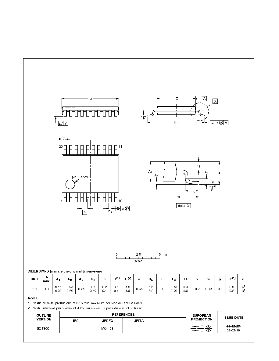
TSSOP20:
plastic thin shrink small outline package; 20 leads; body width 4.4 mm
SOT360-1
Philips Semiconductors
Product data
CBT3245A
Octal bus switch
2003 Jun 27
8
SSOP20:
plastic shrink small outline package; 20 leads;
body width 3.9 mm; lead pitch 0.635 mm
SOT724-1
Philips Semiconductors
Product data
CBT3245A
Octal bus switch
2003 Jun 27
9
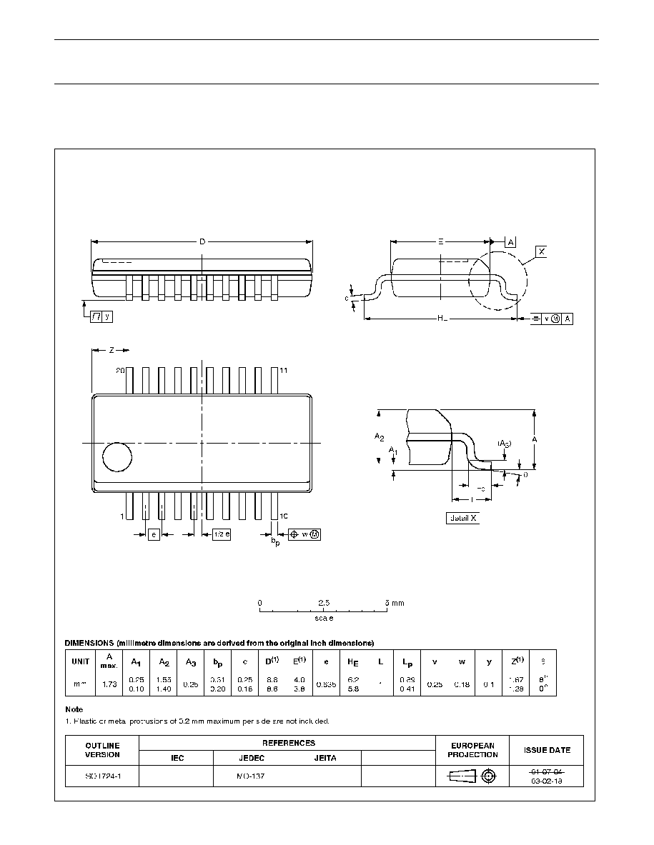
SSOP20:
plastic shrink small outline package; 20 leads; body width 5.3 mm
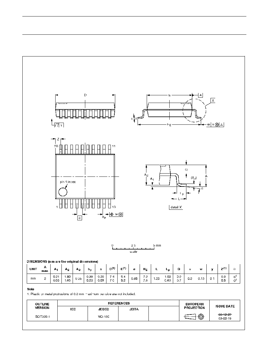
SOT339-1
Philips Semiconductors
Product data
CBT3245A
Octal bus switch
2003 Jun 27
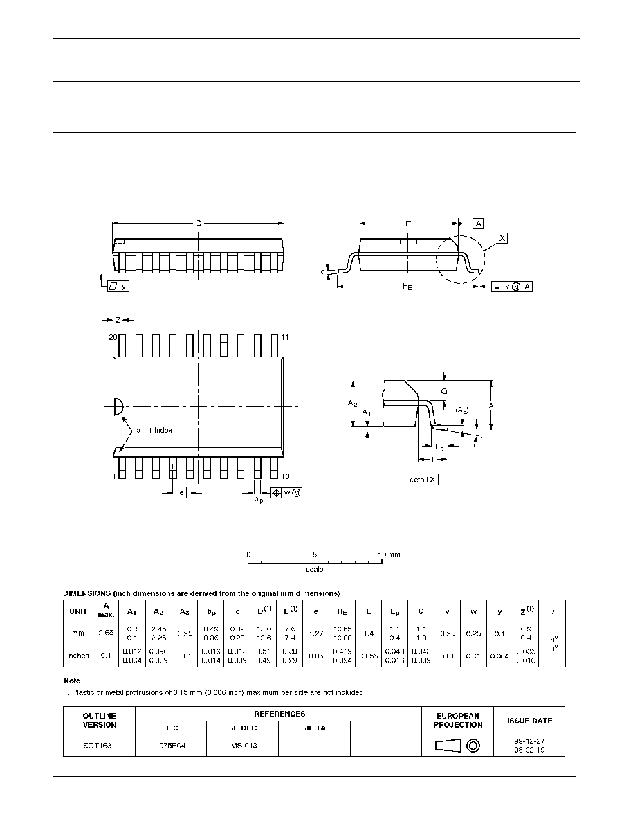
10
SO20:
plastic small outline package; 20 leads; body width 7.5 mm
SOT163-1

Philips Semiconductors
Product data
CBT3245A
Octal bus switch
2003 Jun 27
11
REVISION HISTORY
Rev
Date
Description
_2
20030627
Product data (9397 750 11679); ECN 853-2313 30017 dated 11 Jun 2003.
Supersedes data of 2002 Feb 18 (9397 750 09462).
Modifications:
·
Addition of QSOP and DHVQFN package types.
_1
20020218
Product data (9397 750 09462); ECN 853-2313 27745 of 18 Feb 2002.
Philips Semiconductors
Product data
CBT3245A
Octal bus switch
2003 Jun 27
12
Definitions
Short-form specification -- The data in a short-form specification is extracted from a full data sheet with the same type number and title. For detailed information see
the relevant data sheet or data handbook.
Limiting values definition -- Limiting values given are in accordance with the Absolute Maximum Rating System (IEC 60134). Stress above one or more of the limiting
values may cause permanent damage to the device. These are stress ratings only and operation of the device at these or at any other conditions above those given
in the Characteristics sections of the specification is not implied. Exposure to limiting values for extended periods may affect device reliability.
Application information -- Applications that are described herein for any of these products are for illustrative purposes only. Philips Semiconductors make no
representation or warranty that such applications will be suitable for the specified use without further testing or modification.
Disclaimers
Life support -- These products are not designed for use in life support appliances, devices, or systems where malfunction of these products can reasonably be
expected to result in personal injury. Philips Semiconductors customers using or selling these products for use in such applications do so at their own risk and agree
to fully indemnify Philips Semiconductors for any damages resulting from such application.
Right to make changes -- Philips Semiconductors reserves the right to make changes in the products--including circuits, standard cells, and/or software--described
or contained herein in order to improve design and/or performance. When the product is in full production (status `Production'), relevant changes will be communicated
via a Customer Product/Process Change Notification (CPCN). Philips Semiconductors assumes no responsibility or liability for the use of any of these products, conveys
no license or title under any patent, copyright, or mask work right to these products, and makes no representations or warranties that these products are free from patent,
copyright, or mask work right infringement, unless otherwise specified.
Contact information
For additional information please visit
http://www.semiconductors.philips.com .
Fax: +31 40 27 24825
For sales offices addresses send e-mail to:
sales.addresses@www.semiconductors.philips.com .
Koninklijke Philips Electronics N.V. 2003
All rights reserved. Printed in U.S.A.
Date of release: 06-03
Document order number:
9397 750 11679
Philips
Semiconductors
Data sheet status
[1]
Objective data
Preliminary data
Product data
Product
status
[2] [3]
Development
Qualification
Production
Definitions
This data sheet contains data from the objective specification for product development.
Philips Semiconductors reserves the right to change the specification in any manner without notice.
This data sheet contains data from the preliminary specification. Supplementary data will be published
at a later date. Philips Semiconductors reserves the right to change the specification without notice, in
order to improve the design and supply the best possible product.
This data sheet contains data from the product specification. Philips Semiconductors reserves the
right to make changes at any time in order to improve the design, manufacturing and supply. Relevant
changes will be communicated via a Customer Product/Process Change Notification (CPCN).
Data sheet status
[1] Please consult the most recently issued data sheet before initiating or completing a design.
[2] The product status of the device(s) described in this data sheet may have changed since this data sheet was published. The latest information is available on the Internet at URL
http://www.semiconductors.philips.com.
[3] For data sheets describing multiple type numbers, the highest-level product status determines the data sheet status.
Level
I
II
III
Document Outline
- FEATURES
- DESCRIPTION
- PIN CONFIGURATION SO, SSOP, QSOP, AND TSSOP
- PIN CONFIGURATION DHVQFN
- PIN DESCRIPTION
- ORDERING INFORMATION
- LOGIC SYMBOL
- FUNCTION TABLE
- ABSOLUTE MAXIMUM RATINGS 1, 2
- RECOMMENDED OPERATING CONDITIONS
- DC ELECTRICAL CHARACTERISTICS
- AC CHARACTERISTICS
- AC WAVEFORMS
- TEST CIRCUIT AND WAVEFORMS
- PACKAGE OUTLINE
- SOT764-1
- SOT360-1
- SOT724-1
- SOT339-1
- SOT163-1
- REVISION HISTORY
- Data sheet status
- Definitions
- Disclaimers