CBT3253A
Dual 1-of-4 FET multiplexer/demultiplexer
1.
General description
The CBT3253A is a dual 1-of-4 high-speed TTL-compatible FET
multiplexer/demultiplexer. The low on-resistance of the switch allows inputs to be
connected to outputs without adding propagation delay or generating additional ground
bounce noise.
1OE, 2OE, S0, and S1 select the appropriate B output for the A-input data.
The CBT3253A is characterized for operation from
-
40
∞
C to +85
∞
C.
2.
Features
s
5
switch connection between two ports
s
TTL-compatible input levels
s
Minimal propagation delay through the switch
s
ESD protection exceeds 2000 V HBM per JESD22-A114, 200 V MM per
JESD22-A115 and 1000 V CDM per JESD22-C101
s
Latch-up testing is done to JEDEC Standard JESD78 which exceeds 100 mA
3.
Ordering information
[1]
Also known as QSOP16.
CBT3253A
Dual 1-of-4 FET multiplexer/demultiplexer
Rev. 01 -- 24 October 2005
Product data sheet
Table 1:
Ordering information
T
amb
=
-
40
∞
C to +85
∞
C
Type number
Topside
mark
Package
Name
Description
Version
CBT3253AD
CBT3253AD
SO16
plastic small outline package; 16 leads;
body width 3.9 mm
SOT109-1
CBT3253ADB
C3253A
SSOP16
plastic shrink small outline package;
16 leads; body width 5.3 mm
SOT338-1
CBT3253ADS
CT3253A
SSOP16
[1]
plastic shrink small outline package;
16 leads; body width 3.9 mm;
lead pitch 0.635 mm
SOT519-1
CBT3253APW CT3253A
TSSOP16
plastic thin shrink small outline package;
16 leads; body width 4.4 mm
SOT403-1
9397 750 12919
© Koninklijke Philips Electronics N.V. 2005. All rights reserved.
Product data sheet
Rev. 01 -- 24 October 2005
2 of 16
Philips Semiconductors
CBT3253A
Dual 1-of-4 FET multiplexer/demultiplexer
4.
Functional diagram
Fig 1.
Logic diagram of CBT3253A (positive logic)
002aab828
2B4
13
2B3
12
2B2
11
2B1
10
1B4
3
1B3
4
1B2
5
1B1
6
1A
7
CBT3253A
2A
9
14
S0
2
S1
1
1OE
15
2OE
9397 750 12919
© Koninklijke Philips Electronics N.V. 2005. All rights reserved.
Product data sheet
Rev. 01 -- 24 October 2005
3 of 16
Philips Semiconductors
CBT3253A
Dual 1-of-4 FET multiplexer/demultiplexer
5.
Pinning information
5.1 Pinning
5.2 Pin description
[1]
B outputs are inputs if A inputs are outputs.
Fig 2.
Pin configuration for SO16
Fig 3.
Pin configuration for SSOP16
Fig 4.
Pin configuration for SSOP16
(QSOP16)
Fig 5.
Pin configuration for TSSOP16
CBT3253AD
V
CC
S1
2OE
1B4
S0
1B3
2B4
1B2
2B3
1B1
2B2
1A
2B1
GND
2A
002aab824
1
2
3
4
5
6
7
8
10
9
12
11
14
13
16
15
1OE
S1
2OE
1B4
S0
1B3
2B4
1B2
2B3
1B1
2B2
1A
2B1
2A
1OE
CBT3253ADB
V
CC
GND
002aab825
1
2
3
4
5
6
7
8
10
9
12
11
14
13
16
15
S1
2OE
1B4
S0
1B3
2B4
1B2
2B3
1B1
2B2
1A
2B1
2A
1OE
CBT3253ADS
V
CC
GND
002aab826
1
2
3
4
5
6
7
8
10
9
12
11
14
13
16
15
S1
2OE
1B4
S0
1B3
2B4
1B2
2B3
1B1
2B2
1A
2B1
2A
1OE
GND
CBT3253APW
V
CC
002aab827
1
2
3
4
5
6
7
8
10
9
12
11
14
13
16
15
Table 2:
Pin description
Symbol
Pin
Description
1OE
1
output enable (active LOW)
S1
2
select-control input
1B4, 1B3, 1B2, 1B1
3, 4, 5, 6
B outputs
[1]
1A
7
A input
GND
8
ground (0 V)
2A
9
A input
2B1, 2B2, 2B3, 2B4
10, 11, 12, 13
B outputs
S0
14
select-control input
2OE
15
output enable (active LOW)
V
CC
16
positive supply voltage

9397 750 12919
© Koninklijke Philips Electronics N.V. 2005. All rights reserved.
Product data sheet
Rev. 01 -- 24 October 2005
4 of 16
Philips Semiconductors
CBT3253A
Dual 1-of-4 FET multiplexer/demultiplexer
6.
Functional description
Refer to
Figure 1 "Logic diagram of CBT3253A (positive logic)"
6.1 Function selection
7.
Limiting values
[1]
The input and output negative voltage ratings may be exceeded if the input and output clamp current ratings
are observed.
8.
Recommended operating conditions
Table 3:
Function selection
H = HIGH state; L = LOW state; X = Don't Care
Inputs
Function
1OE
2OE
S1
S0
X
H
X
X
disconnect 1A and 2A
H
X
X
X
disconnect 1A and 2A
L
L
L
L
1A to 1B1 and 2A to 2B1
L
L
L
H
1A to 1B2 and 2A to 2B2
L
L
H
L
1A to 1B3 and 2A to 2B3
L
L
H
H
1A to 1B4 and 2A to 2B4
Table 4:
Limiting values
In accordance with the Absolute Maximum Rating System (IEC 60134).
Symbol
Parameter
Conditions
Min
Max
Unit
V
CC
supply voltage
-
0.5
+7.0
V
V
I
input voltage
-
0.5
[1]
+7.0
V
I
CCC
continuous current through
each V
CC
or GND pin
-
128
mA
I
IK
input clamping current
V
I
< 0 V
-
-
50
mA
T
stg
storage temperature
-
65
+150
∞
C
Table 5:
Operating conditions
All unused control inputs of the device must be held at V
CC
or GND to ensure proper device
operation.
Symbol
Parameter
Conditions
Min
Typ
Max
Unit
V
CC
supply voltage
4.5
-
5.5
V
V
IH
HIGH-state input voltage
2
-
-
V
V
IL
LOW-state input voltage
-
-
0.8
V
T
amb
ambient temperature
operating in free air
-
40
-
+85
∞
C

9397 750 12919
© Koninklijke Philips Electronics N.V. 2005. All rights reserved.
Product data sheet
Rev. 01 -- 24 October 2005
5 of 16
Philips Semiconductors
CBT3253A
Dual 1-of-4 FET multiplexer/demultiplexer
9.
Static characteristics
[1]
All typical values are at V
CC
= 5 V, T
amb
= 25
∞
C.
[2]
This is the increase in supply current for each input that is at the specified TTL voltage level rather than V
CC
or GND.
[3]
Measured by the voltage drop between the A and the B terminals at the indicated current through the switch. ON-state resistance is
determined by the lowest voltage of the two (A or B) terminals.
10. Dynamic characteristics
[1]
The propagation delay is the calculated RC time constant of the typical ON-state resistance of the switch and the specified load
capacitance, when driven by an ideal voltage source (zero output impedance).
[2]
Output enable time to HIGH and LOW level.
[3]
Output disable time from HIGH and LOW level.
Table 6:
Static characteristics
T
amb
=
-
40
∞
C to +85
∞
C
Symbol
Parameter
Conditions
Min
Typ
[1]
Max
Unit
V
IK
input clamping voltage
V
CC
= 4.5 V; I
I
=
-
18 mA
-
-
-
1.2
V
V
pass
pass voltage
V
I
= V
CC
= 5.5 V; I
O
=
-
100
µ
A
3.4
3.6
3.9
V
I
LI
input leakage current
V
CC
= 5 V; V
I
= 5.5 V or GND
-
-
±
1
µ
A
I
CC
quiescent supply current
V
CC
= 5.5 V; I
O
= 0 mA;
V
I
= V
CC
or GND
-
-
3
µ
A
I
CC
additional quiescent supply
current (control inputs)
V
CC
= 5.5 V; one input at 3.4 V;
other inputs at V
CC
or GND
[2]
-
-
2.5
mA
C
i
input capacitance
(control pins)
V
I
= 3 V or 0 V
-
4.5
-
pF
C
io(off)
off-state input/output
capacitance
A port; V
O
= 3 V or 0 V; OE = V
CC
-
23.5
-
pF
B port; V
O
= 3 V or 0 V; OE = V
CC
-
6.5
-
pF
R
on
ON-state resistance
[3]
V
CC
= 4.5 V; V
I
= 0 V; I
I
= 64 mA
-
5
7
V
CC
= 4.5 V; V
I
= 0 V; I
I
= 30 mA
-
5
7
V
CC
= 4.5 V; V
I
= 2.4 V; I
I
=
-
15 mA
-
10
15
Table 7:
Dynamic characteristics
V
CC
= +5.0 V
±
0.5 V; T
amb
=
-
40
∞
C to +85
∞
C; unless otherwise specified.
Symbol
Parameter
Conditions
Min
Typ
Max
Unit
t
PD
propagation delay
from input (nA or nBn) to output (nBn or nA)
[1]
-
-
0.25
ns
from input (Sn) to output (nA or nBn)
1.2
-
6.2
ns
t
en
enable time
[2]
from input (Sn) to output (nA or nBn)
1.3
-
6.3
ns
from input (nOE) to output (nA or nBn)
1.4
-
6.4
ns
t
dis
disable time
[3]
from input (Sn) to output (nA or nBn)
1.1
-
7.2
ns
from input (nOE) to output (nA or nBn)
1.0
-
7
ns
9397 750 12919
© Koninklijke Philips Electronics N.V. 2005. All rights reserved.
Product data sheet
Rev. 01 -- 24 October 2005
6 of 16
Philips Semiconductors
CBT3253A
Dual 1-of-4 FET multiplexer/demultiplexer
10.1 AC waveforms
V
I
= GND to 3.0 V.
t
PLZ
and t
PHZ
are the same as t
dis
.
t
PZL
and t
PZH
are the same as t
en
.
t
PLH
and t
PHL
are the same as t
PD
.
Fig 6.
Input to output propagation delay
(1) Waveform 1 is for an output with internal conditions such that the output is LOW except when
disabled by the output control.
(2) Waveform 2 is for an output with internal conditions such that the output is HIGH except when
disabled by the output control.
Fig 7.
3-state output enable and disable times
002aab665
3.0 V
0 V
V
OH
V
OL
t
PLH
t
PHL
1.5 V
1.5 V
input
output
1.5 V
1.5 V
002aab666
3 V
3.5 V
t
PLZ
1.5 V
1.5 V
output control
(LOW-level enabling)
output
waveform 1
S1 at 7 V
(1)
1.5 V
t
PZL
V
OL
0 V
V
OL
+ 0.3 V
V
OH
0 V
1.5 V
V
OL
-
0.3 V
output
waveform 2
S1 open
(2)
t
PZH
t
PHZ
9397 750 12919
© Koninklijke Philips Electronics N.V. 2005. All rights reserved.
Product data sheet
Rev. 01 -- 24 October 2005
7 of 16
Philips Semiconductors
CBT3253A
Dual 1-of-4 FET multiplexer/demultiplexer
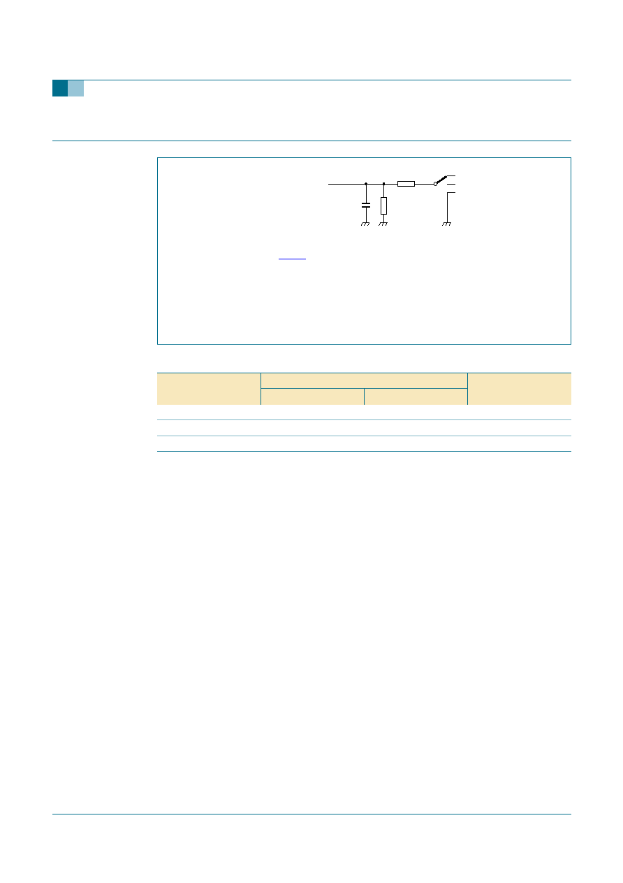
11. Test information
Test data are given in
Table 8
.
All input pulses are supplied by generators having the following characteristics:
PRR
10 MHz; Z
o
= 50
; t
r
2.5 ns; t
f
2.5 ns.
The outputs are measured one at a time with one transition per measurement.
C
L
= load capacitance includes jig and probe capacitance.
R
L
= load resistance.
Fig 8.
Test circuit
Table 8:
Test data
Test
Load
Switch
C
L
R
L
t
PD
50 pF
500
open
t
PLZ
, t
PZL
50 pF
500
7 V
t
PHZ
, t
PZH
50 pF
500
open
CL
50 pF
002aab667
RL
500
from output under test
7 V
open
GND
S1
RL
500
9397 750 12919
© Koninklijke Philips Electronics N.V. 2005. All rights reserved.
Product data sheet
Rev. 01 -- 24 October 2005
8 of 16
Philips Semiconductors
CBT3253A
Dual 1-of-4 FET multiplexer/demultiplexer
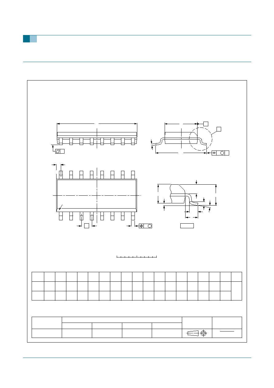
12. Package outline
Fig 9.
Package outline SOT109-1 (SO16)
X
w
M
A
A
1
A
2
b
p
D
H
E
L
p
Q
detail X
E
Z
e
c
L
v
M
A
(A )
3
A
8
9
1
16
y
pin 1 index
UNIT
A
max.
A
1
A
2
A
3
b
p
c
D
(1)
E
(1)
(1)
e
H
E
L
L
p
Q
Z
y
w
v
REFERENCES
OUTLINE
VERSION
EUROPEAN
PROJECTION
ISSUE DATE
IEC
JEDEC
JEITA
mm
inches
1.75
0.25
0.10
1.45
1.25
0.25
0.49
0.36
0.25
0.19
10.0
9.8
4.0
3.8
1.27
6.2
5.8
0.7
0.6
0.7
0.3
8
0
o
o
0.25
0.1
DIMENSIONS (inch dimensions are derived from the original mm dimensions)
Note
1. Plastic or metal protrusions of 0.15 mm (0.006 inch) maximum per side are not included.
1.0
0.4
SOT109-1
99-12-27
03-02-19
076E07
MS-012
0.069
0.010
0.004
0.057
0.049
0.01
0.019
0.014
0.0100
0.0075
0.39
0.38
0.16
0.15
0.05
1.05
0.041
0.244
0.228
0.028
0.020
0.028
0.012
0.01
0.25
0.01
0.004
0.039
0.016
0
2.5
5 mm
scale
SO16: plastic small outline package; 16 leads; body width 3.9 mm
SOT109-1
9397 750 12919
© Koninklijke Philips Electronics N.V. 2005. All rights reserved.
Product data sheet
Rev. 01 -- 24 October 2005
9 of 16
Philips Semiconductors
CBT3253A
Dual 1-of-4 FET multiplexer/demultiplexer
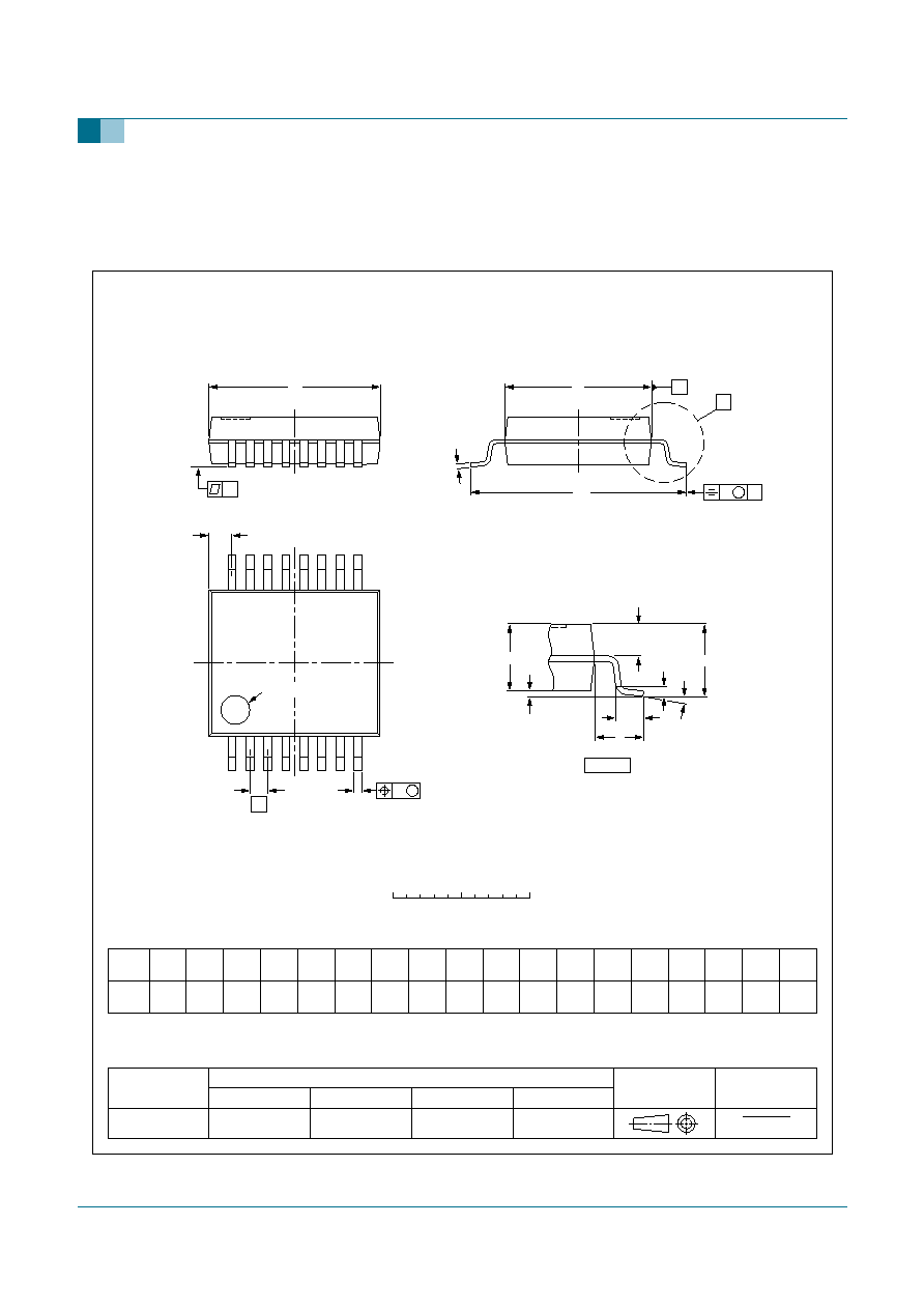
Fig 10. Package outline SOT338-1 (SSOP16)
UNIT
A
1
A
2
A
3
b
p
c
D
(1)
E
(1)
e
H
E
L
L
p
Q
Z
y
w
v
REFERENCES
OUTLINE
VERSION
EUROPEAN
PROJECTION
ISSUE DATE
IEC
JEDEC
JEITA
mm
0.21
0.05
1.80
1.65
0.25
0.38
0.25
0.20
0.09
6.4
6.0
5.4
5.2
0.65
1.25
7.9
7.6
1.03
0.63
0.9
0.7
1.00
0.55
8
0
o
o
0.13
0.2
0.1
DIMENSIONS (mm are the original dimensions)
Note
1. Plastic or metal protrusions of 0.25 mm maximum per side are not included.
SOT338-1
99-12-27
03-02-19
(1)
w
M
b
p
D
H
E
E
Z
e
c
v
M
A
X
A
y
1
8
16
9
A
A
1
A
2
L
p
Q
detail X
L
(A )
3
MO-150
pin 1 index
0
2.5
5 mm
scale
SSOP16: plastic shrink small outline package; 16 leads; body width 5.3 mm
SOT338-1
A
max.
2
9397 750 12919
© Koninklijke Philips Electronics N.V. 2005. All rights reserved.
Product data sheet
Rev. 01 -- 24 October 2005
10 of 16
Philips Semiconductors
CBT3253A
Dual 1-of-4 FET multiplexer/demultiplexer
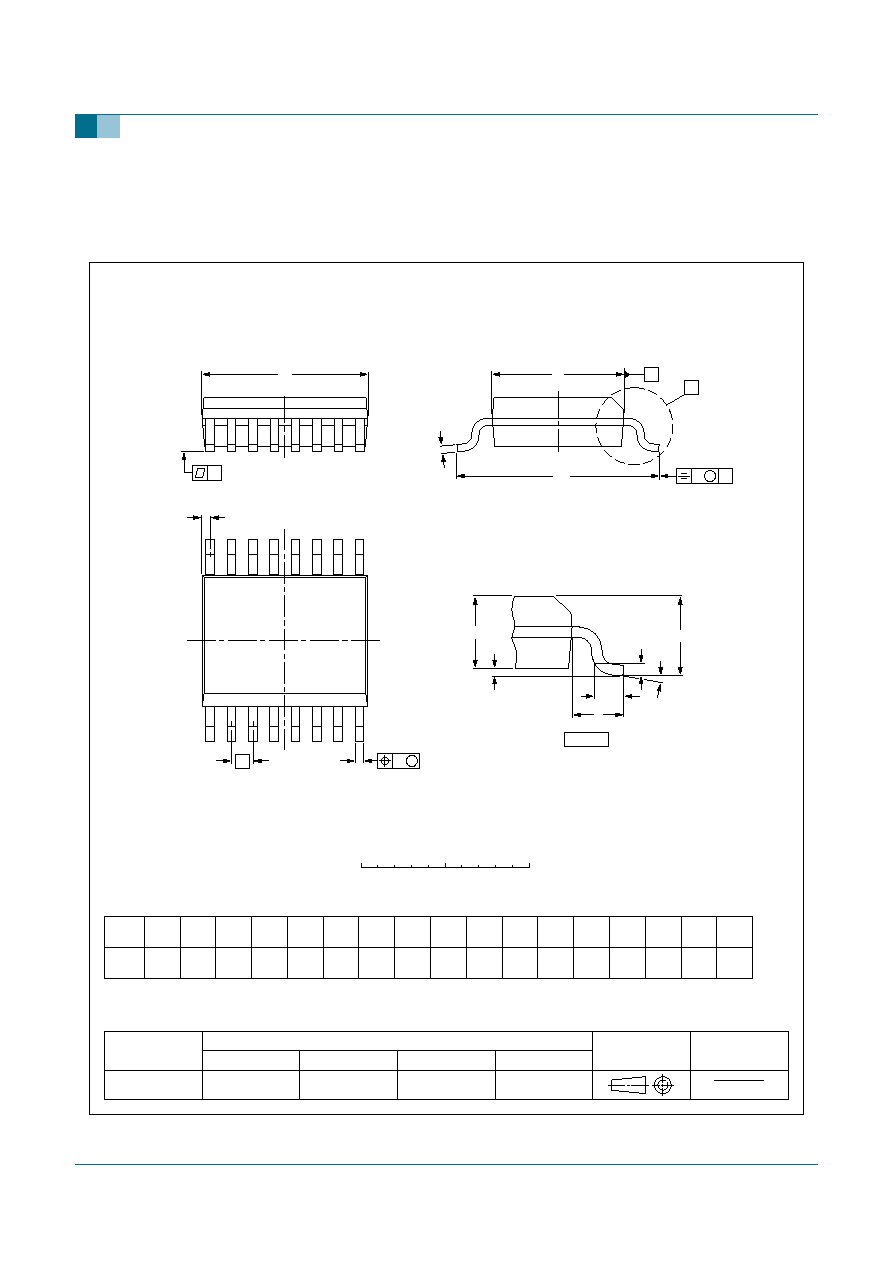
Fig 11. Package outline SOT519-1 (SSOP16)
UNIT
A
1
A
2
A
3
b
p
c
D
(1)
E
(1)
e
H
E
L
L
p
Z
y
w
v
REFERENCES
OUTLINE
VERSION
EUROPEAN
PROJECTION
ISSUE DATE
IEC
JEDEC
JEITA
mm
0.25
0.10
1.55
1.40
0.25
0.31
0.20
0.25
0.18
5.0
4.8
4.0
3.8
0.635
1
6.2
5.8
0.89
0.41
0.18
0.05
8
0
o
o
0.18
0.2
0.09
DIMENSIONS (mm are the original dimensions)
Note
1. Plastic or metal protrusions of 0.2 mm maximum per side are not included.
SOT519-1
99-05-04
03-02-18
(1)
w
M
b
p
D
H
E
E
Z
e
c
v
M
A
X
A
y
1
8
16
9
A
A
1
A
2
L
p
detail X
L
(A )
3
0
2.5
5 mm
scale
SSOP16: plastic shrink small outline package; 16 leads; body width 3.9 mm; lead pitch 0.635 mm
SOT519-1
A
max.
1.73
9397 750 12919
© Koninklijke Philips Electronics N.V. 2005. All rights reserved.
Product data sheet
Rev. 01 -- 24 October 2005
11 of 16
Philips Semiconductors
CBT3253A
Dual 1-of-4 FET multiplexer/demultiplexer
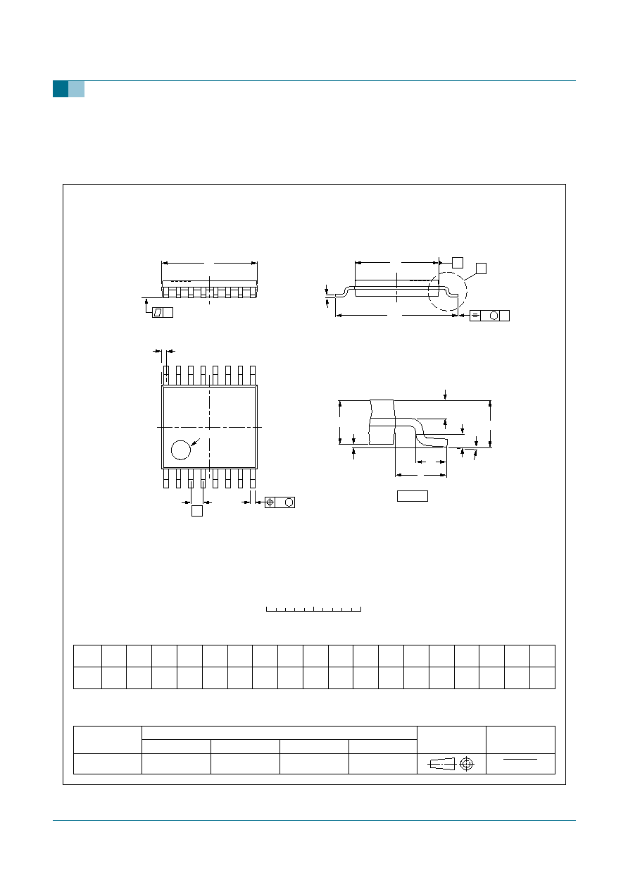
Fig 12. Package outline SOT403-1 (TSSOP16)
UNIT
A
1
A
2
A
3
b
p
c
D
(1)
E
(2)
(1)
e
H
E
L
L
p
Q
Z
y
w
v
REFERENCES
OUTLINE
VERSION
EUROPEAN
PROJECTION
ISSUE DATE
IEC
JEDEC
JEITA
mm
0.15
0.05
0.95
0.80
0.30
0.19
0.2
0.1
5.1
4.9
4.5
4.3
0.65
6.6
6.2
0.4
0.3
0.40
0.06
8
0
o
o
0.13
0.1
0.2
1
DIMENSIONS (mm are the original dimensions)
Notes
1. Plastic or metal protrusions of 0.15 mm maximum per side are not included.
2. Plastic interlead protrusions of 0.25 mm maximum per side are not included.
0.75
0.50
SOT403-1
MO-153
99-12-27
03-02-18
w
M
b
p
D
Z
e
0.25
1
8
16
9
A
A
1
A
2
L
p
Q
detail X
L
(A )
3
H
E
E
c
v
M
A
X
A
y
0
2.5
5 mm
scale
TSSOP16: plastic thin shrink small outline package; 16 leads; body width 4.4 mm
SOT403-1
A
max.
1.1
pin 1 index

9397 750 12919
© Koninklijke Philips Electronics N.V. 2005. All rights reserved.
Product data sheet
Rev. 01 -- 24 October 2005
12 of 16
Philips Semiconductors
CBT3253A
Dual 1-of-4 FET multiplexer/demultiplexer
13. Soldering
13.1 Introduction to soldering surface mount packages
This text gives a very brief insight to a complex technology. A more in-depth account of
soldering ICs can be found in our
Data Handbook IC26; Integrated Circuit Packages
(document order number 9398 652 90011).
There is no soldering method that is ideal for all surface mount IC packages. Wave
soldering can still be used for certain surface mount ICs, but it is not suitable for fine pitch
SMDs. In these situations reflow soldering is recommended.
13.2 Reflow soldering
Reflow soldering requires solder paste (a suspension of fine solder particles, flux and
binding agent) to be applied to the printed-circuit board by screen printing, stencilling or
pressure-syringe dispensing before package placement. Driven by legislation and
environmental forces the worldwide use of lead-free solder pastes is increasing.
Several methods exist for reflowing; for example, convection or convection/infrared
heating in a conveyor type oven. Throughput times (preheating, soldering and cooling)
vary between 100 seconds and 200 seconds depending on heating method.
Typical reflow peak temperatures range from 215
∞
C to 270
∞
C depending on solder paste
material. The top-surface temperature of the packages should preferably be kept:
∑
below 225
∞
C (SnPb process) or below 245
∞
C (Pb-free process)
≠ for all BGA, HTSSON..T and SSOP..T packages
≠ for packages with a thickness
2.5 mm
≠ for packages with a thickness < 2.5 mm and a volume
350 mm
3
so called
thick/large packages.
∑
below 240
∞
C (SnPb process) or below 260
∞
C (Pb-free process) for packages with a
thickness < 2.5 mm and a volume < 350 mm
3
so called small/thin packages.
Moisture sensitivity precautions, as indicated on packing, must be respected at all times.
13.3 Wave soldering
Conventional single wave soldering is not recommended for surface mount devices
(SMDs) or printed-circuit boards with a high component density, as solder bridging and
non-wetting can present major problems.
To overcome these problems the double-wave soldering method was specifically
developed.
If wave soldering is used the following conditions must be observed for optimal results:
∑
Use a double-wave soldering method comprising a turbulent wave with high upward
pressure followed by a smooth laminar wave.
∑
For packages with leads on two sides and a pitch (e):
≠ larger than or equal to 1.27 mm, the footprint longitudinal axis is preferred to be
parallel to the transport direction of the printed-circuit board;

9397 750 12919
© Koninklijke Philips Electronics N.V. 2005. All rights reserved.
Product data sheet
Rev. 01 -- 24 October 2005
13 of 16
Philips Semiconductors
CBT3253A
Dual 1-of-4 FET multiplexer/demultiplexer
≠ smaller than 1.27 mm, the footprint longitudinal axis must be parallel to the
transport direction of the printed-circuit board.
The footprint must incorporate solder thieves at the downstream end.
∑
For packages with leads on four sides, the footprint must be placed at a 45
∞
angle to
the transport direction of the printed-circuit board. The footprint must incorporate
solder thieves downstream and at the side corners.
During placement and before soldering, the package must be fixed with a droplet of
adhesive. The adhesive can be applied by screen printing, pin transfer or syringe
dispensing. The package can be soldered after the adhesive is cured.
Typical dwell time of the leads in the wave ranges from 3 seconds to 4 seconds at 250
∞
C
or 265
∞
C, depending on solder material applied, SnPb or Pb-free respectively.
A mildly-activated flux will eliminate the need for removal of corrosive residues in most
applications.
13.4 Manual soldering
Fix the component by first soldering two diagonally-opposite end leads. Use a low voltage
(24 V or less) soldering iron applied to the flat part of the lead. Contact time must be
limited to 10 seconds at up to 300
∞
C.
When using a dedicated tool, all other leads can be soldered in one operation within
2 seconds to 5 seconds between 270
∞
C and 320
∞
C.
13.5 Package related soldering information
[1]
For more detailed information on the BGA packages refer to the
(LF)BGA Application Note (AN01026);
order a copy from your Philips Semiconductors sales office.
[2]
All surface mount (SMD) packages are moisture sensitive. Depending upon the moisture content, the
maximum temperature (with respect to time) and body size of the package, there is a risk that internal or
external package cracks may occur due to vaporization of the moisture in them (the so called popcorn
effect). For details, refer to the Drypack information in the
Data Handbook IC26; Integrated Circuit
Packages; Section: Packing Methods.
[3]
These transparent plastic packages are extremely sensitive to reflow soldering conditions and must on no
account be processed through more than one soldering cycle or subjected to infrared reflow soldering with
peak temperature exceeding 217
∞
C
±
10
∞
C measured in the atmosphere of the reflow oven. The package
body peak temperature must be kept as low as possible.
Table 9:
Suitability of surface mount IC packages for wave and reflow soldering methods
Package
[1]
Soldering method
Wave
Reflow
[2]
BGA, HTSSON..T
[3]
, LBGA, LFBGA, SQFP,
SSOP..T
[3]
, TFBGA, VFBGA, XSON
not suitable
suitable
DHVQFN, HBCC, HBGA, HLQFP, HSO, HSOP,
HSQFP, HSSON, HTQFP, HTSSOP, HVQFN,
HVSON, SMS
not suitable
[4]
suitable
PLCC
[5]
, SO, SOJ
suitable
suitable
LQFP, QFP, TQFP
not recommended
[5] [6]
suitable
SSOP, TSSOP, VSO, VSSOP
not recommended
[7]
suitable
CWQCCN..L
[8]
, PMFP
[9]
, WQCCN..L
[8]
not suitable
not suitable

9397 750 12919
© Koninklijke Philips Electronics N.V. 2005. All rights reserved.
Product data sheet
Rev. 01 -- 24 October 2005
14 of 16
Philips Semiconductors
CBT3253A
Dual 1-of-4 FET multiplexer/demultiplexer
[4]
These packages are not suitable for wave soldering. On versions with the heatsink on the bottom side, the
solder cannot penetrate between the printed-circuit board and the heatsink. On versions with the heatsink
on the top side, the solder might be deposited on the heatsink surface.
[5]
If wave soldering is considered, then the package must be placed at a 45
∞
angle to the solder wave
direction. The package footprint must incorporate solder thieves downstream and at the side corners.
[6]
Wave soldering is suitable for LQFP, QFP and TQFP packages with a pitch (e) larger than 0.8 mm; it is
definitely not suitable for packages with a pitch (e) equal to or smaller than 0.65 mm.
[7]
Wave soldering is suitable for SSOP, TSSOP, VSO and VSSOP packages with a pitch (e) equal to or larger
than 0.65 mm; it is definitely not suitable for packages with a pitch (e) equal to or smaller than 0.5 mm.
[8]
Image sensor packages in principle should not be soldered. They are mounted in sockets or delivered
pre-mounted on flex foil. However, the image sensor package can be mounted by the client on a flex foil by
using a hot bar soldering process. The appropriate soldering profile can be provided on request.
[9]
Hot bar soldering or manual soldering is suitable for PMFP packages.
14. Abbreviations
15. Revision history
Table 10:
Abbreviations
Acronym
Description
CDM
Charged Device Model
ESD
ElectroStatic Discharge
FET
Field-Effect Transistor
HBM
Human Body Model
MM
Machine Model
PRR
Pulse Rate Repetition
TTL
Transistor-Transistor Logic
Table 11:
Revision history
Document ID
Release date
Data sheet status
Change notice
Doc. number
Supersedes
CBT3253A_1
20051024
Product data sheet
-
9397 750 12919
-

Philips Semiconductors
CBT3253A
Dual 1-of-4 FET multiplexer/demultiplexer
9397 750 12919
© Koninklijke Philips Electronics N.V. 2005. All rights reserved.
Product data sheet
Rev. 01 -- 24 October 2005
15 of 16
16. Data sheet status
[1]
Please consult the most recently issued data sheet before initiating or completing a design.
[2]
The product status of the device(s) described in this data sheet may have changed since this data sheet was published. The latest information is available on the Internet at
URL http://www.semiconductors.philips.com.
[3]
For data sheets describing multiple type numbers, the highest-level product status determines the data sheet status.
17. Definitions
Short-form specification -- The data in a short-form specification is
extracted from a full data sheet with the same type number and title. For
detailed information see the relevant data sheet or data handbook.
Limiting values definition -- Limiting values given are in accordance with
the Absolute Maximum Rating System (IEC 60134). Stress above one or
more of the limiting values may cause permanent damage to the device.
These are stress ratings only and operation of the device at these or at any
other conditions above those given in the Characteristics sections of the
specification is not implied. Exposure to limiting values for extended periods
may affect device reliability.
Application information -- Applications that are described herein for any
of these products are for illustrative purposes only. Philips Semiconductors
make no representation or warranty that such applications will be suitable for
the specified use without further testing or modification.
18. Disclaimers
Life support -- These products are not designed for use in life support
appliances, devices, or systems where malfunction of these products can
reasonably be expected to result in personal injury. Philips Semiconductors
customers using or selling these products for use in such applications do so
at their own risk and agree to fully indemnify Philips Semiconductors for any
damages resulting from such application.
Right to make changes -- Philips Semiconductors reserves the right to
make changes in the products - including circuits, standard cells, and/or
software - described or contained herein in order to improve design and/or
performance. When the product is in full production (status `Production'),
relevant changes will be communicated via a Customer Product/Process
Change Notification (CPCN). Philips Semiconductors assumes no
responsibility or liability for the use of any of these products, conveys no
license or title under any patent, copyright, or mask work right to these
products, and makes no representations or warranties that these products are
free from patent, copyright, or mask work right infringement, unless otherwise
specified.
19. Trademarks
Notice -- All referenced brands, product names, service names and
trademarks are the property of their respective owners.
20. Contact information
For additional information, please visit: http://www.semiconductors.philips.com
For sales office addresses, send an email to: sales.addresses@www.semiconductors.philips.com
Level
Data sheet status
[1]
Product status
[2] [3]
Definition
I
Objective data
Development
This data sheet contains data from the objective specification for product development. Philips
Semiconductors reserves the right to change the specification in any manner without notice.
II
Preliminary data
Qualification
This data sheet contains data from the preliminary specification. Supplementary data will be published
at a later date. Philips Semiconductors reserves the right to change the specification without notice, in
order to improve the design and supply the best possible product.
III
Product data
Production
This data sheet contains data from the product specification. Philips Semiconductors reserves the
right to make changes at any time in order to improve the design, manufacturing and supply. Relevant
changes will be communicated via a Customer Product/Process Change Notification (CPCN).

© Koninklijke Philips Electronics N.V. 2005
All rights are reserved. Reproduction in whole or in part is prohibited without the prior
written consent of the copyright owner. The information presented in this document does
not form part of any quotation or contract, is believed to be accurate and reliable and may
be changed without notice. No liability will be accepted by the publisher for any
consequence of its use. Publication thereof does not convey nor imply any license under
patent- or other industrial or intellectual property rights.
Date of release: 24 October 2005
Document number: 9397 750 12919
Published in The Netherlands
Philips Semiconductors
CBT3253A
Dual 1-of-4 FET multiplexer/demultiplexer
21. Contents
1
General description . . . . . . . . . . . . . . . . . . . . . . 1
2
Features . . . . . . . . . . . . . . . . . . . . . . . . . . . . . . . 1
3
Ordering information . . . . . . . . . . . . . . . . . . . . . 1
4
Functional diagram . . . . . . . . . . . . . . . . . . . . . . 2
5
Pinning information . . . . . . . . . . . . . . . . . . . . . . 3
5.1
Pinning . . . . . . . . . . . . . . . . . . . . . . . . . . . . . . . 3
5.2
Pin description . . . . . . . . . . . . . . . . . . . . . . . . . 3
6
Functional description . . . . . . . . . . . . . . . . . . . 4
6.1
Function selection. . . . . . . . . . . . . . . . . . . . . . . 4
7
Limiting values. . . . . . . . . . . . . . . . . . . . . . . . . . 4
8
Recommended operating conditions. . . . . . . . 4
9
Static characteristics. . . . . . . . . . . . . . . . . . . . . 5
10
Dynamic characteristics . . . . . . . . . . . . . . . . . . 5
10.1
AC waveforms. . . . . . . . . . . . . . . . . . . . . . . . . . 6
11
Test information . . . . . . . . . . . . . . . . . . . . . . . . . 7
12
Package outline . . . . . . . . . . . . . . . . . . . . . . . . . 8
13
Soldering . . . . . . . . . . . . . . . . . . . . . . . . . . . . . 12
13.1
Introduction to soldering surface mount
packages . . . . . . . . . . . . . . . . . . . . . . . . . . . . 12
13.2
Reflow soldering . . . . . . . . . . . . . . . . . . . . . . . 12
13.3
Wave soldering . . . . . . . . . . . . . . . . . . . . . . . . 12
13.4
Manual soldering . . . . . . . . . . . . . . . . . . . . . . 13
13.5
Package related soldering information . . . . . . 13
14
Abbreviations . . . . . . . . . . . . . . . . . . . . . . . . . . 14
15
Revision history . . . . . . . . . . . . . . . . . . . . . . . . 14
16
Data sheet status . . . . . . . . . . . . . . . . . . . . . . . 15
17
Definitions . . . . . . . . . . . . . . . . . . . . . . . . . . . . 15
18
Disclaimers . . . . . . . . . . . . . . . . . . . . . . . . . . . . 15
19
Trademarks. . . . . . . . . . . . . . . . . . . . . . . . . . . . 15
20
Contact information . . . . . . . . . . . . . . . . . . . . 15
Document Outline