 | ÐлекÑÑоннÑй компоненÑ: CGY2021G | СкаÑаÑÑ:  PDF PDF  ZIP ZIP |
Äîêóìåíòàöèÿ è îïèñàíèÿ www.docs.chipfind.ru
DATA SHEET
Preliminary specification
Supersedes data of 1996 Oct 15
File under Integrated Circuits, IC17
1997 Apr 03
INTEGRATED CIRCUITS
CGY2021G
DCS/PCS 2 W power amplifier
1997 Apr 03
2
Philips Semiconductors
Preliminary specification
DCS/PCS 2 W power amplifier
CGY2021G
FEATURES
·
Power Amplifier (PA) overall efficiency 50% (DCS)
·
34 dB gain
·
0 dBm input power
·
Gain control range >50 dB
·
Integrated power sensor driver
·
Low output noise floor of PA <
-
121 dBm/Hz in
DCS/PCS RX band
·
Wide operating temperature range
-
20 to +85
°
C
·
LQFP 48-pin package
·
Compatible with power ramping controller PCA5077 and
GaAs PA power modulator UBA1710.
APPLICATIONS
·
Hand-held transceivers for DCS/PCS applications
(DCS: 1710 to 1785 MHz and PCS:
1850 to 1910 MHz)
·
1800 MHz Time Division Multiple Access (TDMA)
systems.
GENERAL DESCRIPTION
The CGY2021G is a DCS/PCS class 1 GaAs Monolithic
Microwave Integrated Circuit (MMIC) power amplifier
specifically designed to operate at 4.8 V battery supply.
The chip also includes a power sensor driver so that no
directional coupler is required in the power control loop.
The PA requires only a simple low-pass filter to comply
with the DCS/PCS transmit spurious specification. It can
be switched off and its power controlled by monitoring the
actual drain voltage applied to the amplifier stages.
QUICK REFERENCE DATA
Note
1. For conditions, see Chapters "AC characteristics" and "DC characteristics".
ORDERING INFORMATION
SYMBOL
PARAMETER
(1)
MIN.
TYP.
MAX.
UNIT
V
DD
positive supply voltage
-
4.5
-
V
I
DD
positive peak supply current
-
1.4
-
A
P
o(max)
maximum output power
-
34
-
dBm
T
amb
operating ambient temperature
-
20
-
+85
°
C
TYPE
NUMBER
PACKAGE
NAME
DESCRIPTION
VERSION
CGY2021G
LQFP48
plastic low profile quad flat package; 48 leads; body 7
×
7
×
1.4 mm
SOT313-2
1997 Apr 03
3
Philips Semiconductors
Preliminary specification
DCS/PCS 2 W power amplifier
CGY2021G
BLOCK DIAGRAM
PINNING
SYMBOL
PIN
DESCRIPTION
GND
1 to 5
ground
RFO/V
DD4
6 to 8
PA output and fourth stage supply voltage
GND
9 to 17
ground
DETO/V
DD5
18
power sensor output and supply voltage
V
GG2
19
third and fourth stage negative gate supply voltage
GND
20 to 26
ground
RFI
27
PA input
GND
28
ground
V
DD1
29
first stage supply voltage
GND
30
ground
V
GG1
31
first and second stage negative gate supply voltage
GND
32
ground
V
DD2
33
second stage supply voltage
GND
34 to 41
ground
V
DD3
42
third stage supply voltage
GND
43 to 48
ground
Fig.1 Block diagram.
(1) Ground pins 1 to 5, 9 to 17, 20 to 26, 28, 30, 32, 34 to 41 and 43 to 48.
handbook, full pagewidth
CGY2021G
MGD771
(1)
6,7,8
18
29
33
42
27
GND
SENSOR
DRIVER
VGG2
RFO/VDD4
VDD1
VDD2
VDD3
RFI
DETO/VDD5
31
VGG1
19
1997 Apr 03
4
Philips Semiconductors
Preliminary specification
DCS/PCS 2 W power amplifier
CGY2021G
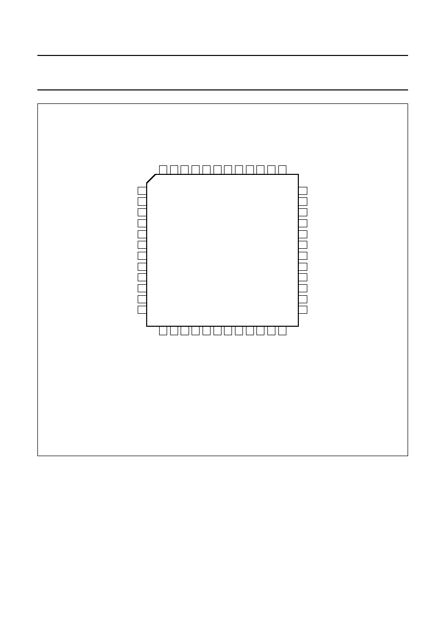
Fig.2 Pin configuration.
handbook, full pagewidth
1
2
3
4
5
6
7
8
9
10
11
36
35
34
33
32
31
30
29
28
27
26
13
14
15
16
17
18
19
20
21
22
23
48
47
46
45
44
43
42
41
40
39
38
12
24
37
25
CGY2021G
MGD770
GND
GND
GND
VDD2
VGG1
GND
VDD1
GND
RFI
GND
GND
GND
GND
GND
GND
GND
RFO/VDD4
RFO/VDD4
GND
GND
GND
GND
GND
GND
GND
GND
GND
GND
V
DD3
GND
GND
GND
GND
GND
GND
RFO/VDD4
GND
GND
GND
GND
DETO/V
DD5
V
GG2
GND
GND
GND
GND
GND
GND
1997 Apr 03
5
Philips Semiconductors
Preliminary specification
DCS/PCS 2 W power amplifier
CGY2021G
FUNCTIONAL DESCRIPTION
Operating conditions
The CGY2021G is designed to meet the European
Telecommunications Standards Institute (ETSI) DCS
documents, the ETS 300 577 specification, which are
defined as follows:
·
t
on
= 542.8
µ
s
·
T = 4.3 ms
·
Duty cycle = 1/8.
This amplifier is specifically designed for pulse operation
allowing the use of a LQFP48 plastic package.
Power amplifier
The Power Amplifier (PA) consists of four cascaded gain
stages with an open-drain configuration. Each drain has to
be loaded externally by an adequate reactive circuit which
also has to be a DC path to the supply.
The amplifier bias is set by using a negative voltage
applied at pins V
GG1
and V
GG2
. This negative voltage must
be present before the supply voltage is applied to the
drains to avoid current overstress of the amplifier.
Power sensor driver
The power sensor driver is a buffer amplifier that delivers
an output signal at the DETO pin which is proportional to
the amplifier power. This signal can be detected by
external diodes for power control purpose. As the sensor
signal is taken from the input of the last stage of the PA,
it is isolated from disturbances at the output by the reverse
isolation of the PA output stage. An impedance mismatch
at the PA output therefore does not significantly influence
the signal delivered by the power sensor as this normally
occurs when power sense is made using a directional
coupler. Consequently, the cost and space of using a
directional coupler are saved.
LIMITING VALUES
In accordance with the Absolute Maximum Rating System (IEC 134); general operating conditions applied.
THERMAL CHARACTERISTICS
General operating conditions applied.
Note
1. This thermal resistance is a typical value and is measured under DCS/PCS pulse conditions.
SYMBOL
PARAMETER
MIN.
MAX.
UNIT
V
DD
positive supply voltage
-
7
V
V
GG
negative supply voltage
-
-
10
V
T
j(max)
maximum operating junction temperature
-
150
°
C
T
stg
IC storage temperature
-
150
°
C
P
tot
total power dissipation
-
1.3
W
SYMBOL
PARAMETER
VALUE
UNIT
R
th j-c
thermal resistance from junction to case; note 1
45
K/W
1997 Apr 03
6
Philips Semiconductors
Preliminary specification
DCS/PCS 2 W power amplifier
CGY2021G
DC CHARACTERISTICS
V
DD
= 4.5 V; T
amb
= 25
°
C; peak current values during burst; general operating conditions applied; unless otherwise
specified.
Note
1. The negative bias V
GG
must be applied 10
µ
s before the power amplifier is switched on, and must remain applied
until the power amplifier has been switched off.
SYMBOL
PARAMETER
CONDITIONS
MIN.
TYP.
MAX.
UNIT
Pins RFO/V
DD4,
V
DD3
, V
DD2
, V
DD1
and DETO/V
DD5
V
DD
positive supply voltage
-
4.5
-
V
I
DD
positive peak supply current
-
1.4
-
A
Pins V
GG1
and V
GG2
V
GG1
negative supply voltage
note 1
-
-
1.6
-
V
V
GG2
negative supply voltage
note 1
-
-
1.6
-
V
I
GG1
+ I
GG2
negative peak supply current
-
-
2
mA
1997 Apr 03
7
Philips Semiconductors
Preliminary specification
DCS/PCS 2 W power amplifier
CGY2021G
AC CHARACTERISTICS
V
DD
= 4.5 V; T
amb
= 25
°
C; general operating conditions applied; unless otherwise specified.
Measured and guaranteed on CGY2021G evaluation board.
Notes
1. Including the 82
resistor connected in parallel at the power amplifier input on the evaluation board.
2. The device is adjusted to provide nominal value of load power into a 50
load. The device is switched off and a 6 : 1
load replaces the 50
load. The device is switched on and the phase of the 6 : 1 load is varied
360 electrical degrees during a 60 seconds test period.
SYMBOL
PARAMETER
CONDITIONS
MIN.
TYP.
MAX.
UNIT
Power amplifier
P
i
input power
-
2
-
+2
dBm
S
11
input return loss
50
source; note 1
-
-
-
10
dB
f
RF
RF frequency range
DCS
1710
-
1785
MHz
PCS
1850
-
1910
MHz
P
o(max)
maximum output power
T
amb
= 25
°
C; V
DD
= 4.5 V
33
34
-
dBm
T
amb
=
-
20 to +85
°
C; V
DD
= 4.2 V
31
-
-
dBm
efficiency
DCS; at P
o(max)
40
50
-
%
PCS; at P
o(max)
-
47
-
%
R
S
optimum series load resistance
-
6
-
C
S
optimum series load
capacitance
-
11
-
pF
P
o(off)
isolation
PA OFF; P
i
= 0 dBm
-
-
50
-
dBm
N
RX
output noise in RX band
-
-
-
121
dBm/Hz
H2
2nd harmonic level
-
-
40
-
dBc
H3
3rd harmonic level
-
-
35
-
dBc
Stab
stability
note 2
-
-
-
50
dBc
Power sensor driver
P
o(DET)
sensor driver output power
R
L
= 100
; relative to PA output
power into 50
load
-
-
25
-
dBc
1997 Apr 03
8
Philips Semiconductors
Preliminary specification
DCS/PCS 2 W power amplifier
CGY2021G
APPLICATION INFORMATION
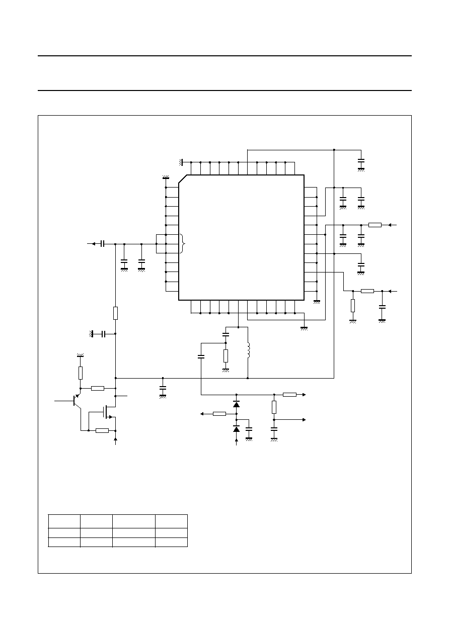
Fig.3 Evaluation board schematic.
handbook, full pagewidth
1
2
3
4
5
6
7
8
9
10
11
48 47 46 45 44 43 42 41 40 39 38 37
12
MGD772
13 14 15 16 17 18
BAS70
BAS70
19 20 21 22 23 24
1 k
1 k
560
1 k
39 pF
100
180
39
-
90
µ
A
12 pF
12 pF
0.8 to 3 V
BSR14
PHP109
6
nH
1 nF
1.25 V
36
35
34
33
32
31
30
29
28
27
26
25
10
pF
1 nF
100
pF
1.5
pF
22
pF
1
nF
C2
(3)
C3
(3)
C1
(3)
10 nF
DC output
Vdiode
Vcontrol
VDD
Vbat
3.6 V
PA
output
-
1.6 V
10 pF
CGY2021G
VGG1
VGG
RFO/VDD4
VDD3
VDD2
VDD1
VGG2
RFI
DETO
10
pF
47
TRL2
(2)
82
PA
input
TRL1
(1)
All capacitors are type: SMD0603.
Thickness: 0.8 mm; substrate: FR4;
r
= 4.7.
(1) TRL1: width = 0.3 mm; length = 16 mm.
(2) TRL2: width = 0.5 mm; length = 10 mm.
(3) the component values are:
SYSTEM
C1 (pF)
C2 (pF)
C3 (pF)
DCS
2.2
1.8
2.2
PCS
1.5
1.5
2.2
1.8
1.2
1997 Apr 03
9
Philips Semiconductors
Preliminary specification
DCS/PCS 2 W power amplifier
CGY2021G
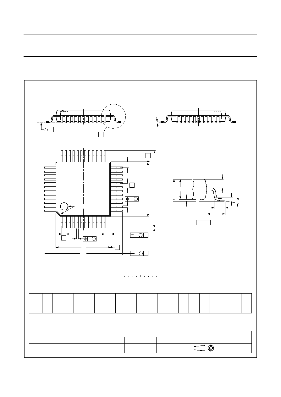
PACKAGE OUTLINE
UNIT
A
max.
A
1
A
2
A
3
b
p
c
E
(1)
e
H
E
L
L
p
Q
Z
y
w
v
REFERENCES
OUTLINE
VERSION
EUROPEAN
PROJECTION
ISSUE DATE
IEC
JEDEC
EIAJ
mm
1.60
0.20
0.05
1.45
1.35
0.25
0.27
0.17
0.18
0.12
7.1
6.9
0.5
9.15
8.85
0.69
0.59
0.95
0.55
7
0
o
o
0.12
0.1
0.2
1.0
DIMENSIONS (mm are the original dimensions)
Note
1. Plastic or metal protrusions of 0.25 mm maximum per side are not included.
0.75
0.45
SOT313-2
93-06-15
94-12-19
D
(1)
(1)
(1)
7.1
6.9
H
D
9.15
8.85
E
Z
0.95
0.55
D
b
p
e
E
B
12
D
H
b
p
E
H
v
M
B
D
ZD
A
Z E
e
v
M
A
1
48
37
36
25
24
13
A
1
A
L
p
Q
detail X
L
(A )
3
A
2
X
y
c
w
M
w
M
0
2.5
5 mm
scale
pin 1 index
LQFP48: plastic low profile quad flat package; 48 leads; body 7 x 7 x 1.4 mm
SOT313-2

1997 Apr 03
10
Philips Semiconductors
Preliminary specification
DCS/PCS 2 W power amplifier
CGY2021G
SOLDERING
Introduction
There is no soldering method that is ideal for all IC
packages. Wave soldering is often preferred when
through-hole and surface mounted components are mixed
on one printed-circuit board. However, wave soldering is
not always suitable for surface mounted ICs, or for
printed-circuits with high population densities. In these
situations reflow soldering is often used.
This text gives a very brief insight to a complex technology.
A more in-depth account of soldering ICs can be found in
our
"IC Package Databook" (order code 9398 652 90011).
Reflow soldering
Reflow soldering techniques are suitable for all LQFP
packages.
Reflow soldering requires solder paste (a suspension of
fine solder particles, flux and binding agent) to be applied
to the printed-circuit board by screen printing, stencilling or
pressure-syringe dispensing before package placement.
Several techniques exist for reflowing; for example,
thermal conduction by heated belt. Dwell times vary
between 50 and 300 seconds depending on heating
method. Typical reflow temperatures range from
215 to 250
°
C.
Preheating is necessary to dry the paste and evaporate
the binding agent. Preheating duration: 45 minutes at
45
°
C.
Wave soldering
Wave soldering is not recommended for LQFP packages.
This is because of the likelihood of solder bridging due to
closely-spaced leads and the possibility of incomplete
solder penetration in multi-lead devices.
If wave soldering cannot be avoided, the following
conditions must be observed:
·
A double-wave (a turbulent wave with high upward
pressure followed by a smooth laminar wave)
soldering technique should be used.
·
The footprint must be at an angle of 45
°
to the board
direction and must incorporate solder thieves
downstream and at the side corners.
Even with these conditions, do not consider wave
soldering LQFP packages LQFP48 (SOT313-2),
LQFP64 (SOT314-2) or LQFP80 (SOT315-1).
During placement and before soldering, the package must
be fixed with a droplet of adhesive. The adhesive can be
applied by screen printing, pin transfer or syringe
dispensing. The package can be soldered after the
adhesive is cured.
Maximum permissible solder temperature is 260
°
C, and
maximum duration of package immersion in solder is
10 seconds, if cooled to less than 150
°
C within
6 seconds. Typical dwell time is 4 seconds at 250
°
C.
A mildly-activated flux will eliminate the need for removal
of corrosive residues in most applications.
Repairing soldered joints
Fix the component by first soldering two diagonally-
opposite end leads. Use only a low voltage soldering iron
(less than 24 V) applied to the flat part of the lead. Contact
time must be limited to 10 seconds at up to 300
°
C. When
using a dedicated tool, all other leads can be soldered in
one operation within 2 to 5 seconds between
270 and 320
°
C.
1997 Apr 03
11
Philips Semiconductors
Preliminary specification
DCS/PCS 2 W power amplifier
CGY2021G
DEFINITIONS
LIFE SUPPORT APPLICATIONS
These products are not designed for use in life support appliances, devices, or systems where malfunction of these
products can reasonably be expected to result in personal injury. Philips customers using or selling these products for
use in such applications do so at their own risk and agree to fully indemnify Philips for any damages resulting from such
improper use or sale.
Data sheet status
Objective specification
This data sheet contains target or goal specifications for product development.
Preliminary specification
This data sheet contains preliminary data; supplementary data may be published later.
Product specification
This data sheet contains final product specifications.
Short-form specification
The data in this specification is extracted from a full data sheet with the same type
number and title. For detailed information see the relevant data sheet or data handbook.
Limiting values
Limiting values given are in accordance with the Absolute Maximum Rating System (IEC 134). Stress above one or
more of the limiting values may cause permanent damage to the device. These are stress ratings only and operation
of the device at these or at any other conditions above those given in the Characteristics sections of the specification
is not implied. Exposure to limiting values for extended periods may affect device reliability.
Application information
Where application information is given, it is advisory and does not form part of the specification.

Internet: http://www.semiconductors.philips.com
Philips Semiconductors a worldwide company
© Philips Electronics N.V. 1997
SCA54
All rights are reserved. Reproduction in whole or in part is prohibited without the prior written consent of the copyright owner.
The information presented in this document does not form part of any quotation or contract, is believed to be accurate and reliable and may be changed
without notice. No liability will be accepted by the publisher for any consequence of its use. Publication thereof does not convey nor imply any license
under patent- or other industrial or intellectual property rights.
Netherlands: Postbus 90050, 5600 PB EINDHOVEN, Bldg. VB,
Tel. +31 40 27 82785, Fax. +31 40 27 88399
New Zealand: 2 Wagener Place, C.P.O. Box 1041, AUCKLAND,
Tel. +64 9 849 4160, Fax. +64 9 849 7811
Norway: Box 1, Manglerud 0612, OSLO,
Tel. +47 22 74 8000, Fax. +47 22 74 8341
Philippines: Philips Semiconductors Philippines Inc.,
106 Valero St. Salcedo Village, P.O. Box 2108 MCC, MAKATI,
Metro MANILA, Tel. +63 2 816 6380, Fax. +63 2 817 3474
Poland: Ul. Lukiska 10, PL 04-123 WARSZAWA,
Tel. +48 22 612 2831, Fax. +48 22 612 2327
Portugal: see Spain
Romania: see Italy
Russia: Philips Russia, Ul. Usatcheva 35A, 119048 MOSCOW,
Tel. +7 095 755 6918, Fax. +7 095 755 6919
Singapore: Lorong 1, Toa Payoh, SINGAPORE 1231,
Tel. +65 350 2538, Fax. +65 251 6500
Slovakia: see Austria
Slovenia: see Italy
South Africa: S.A. PHILIPS Pty Ltd., 195-215 Main Road Martindale,
2092 JOHANNESBURG, P.O. Box 7430 Johannesburg 2000,
Tel. +27 11 470 5911, Fax. +27 11 470 5494
South America: Rua do Rocio 220, 5th floor, Suite 51,
04552-903 São Paulo, SÃO PAULO - SP, Brazil,
Tel. +55 11 821 2333, Fax. +55 11 829 1849
Spain: Balmes 22, 08007 BARCELONA,
Tel. +34 3 301 6312, Fax. +34 3 301 4107
Sweden: Kottbygatan 7, Akalla, S-16485 STOCKHOLM,
Tel. +46 8 632 2000, Fax. +46 8 632 2745
Switzerland: Allmendstrasse 140, CH-8027 ZÜRICH,
Tel. +41 1 488 2686, Fax. +41 1 481 7730
Taiwan: Philips Semiconductors, 6F, No. 96, Chien Kuo N. Rd., Sec. 1,
TAIPEI, Taiwan Tel. +886 2 2134 2865, Fax. +886 2 2134 2874
Thailand: PHILIPS ELECTRONICS (THAILAND) Ltd.,
209/2 Sanpavuth-Bangna Road Prakanong, BANGKOK 10260,
Tel. +66 2 745 4090, Fax. +66 2 398 0793
Turkey: Talatpasa Cad. No. 5, 80640 GÜLTEPE/ISTANBUL,
Tel. +90 212 279 2770, Fax. +90 212 282 6707
Ukraine: PHILIPS UKRAINE, 4 Patrice Lumumba str., Building B, Floor 7,
252042 KIEV, Tel. +380 44 264 2776, Fax. +380 44 268 0461
United Kingdom: Philips Semiconductors Ltd., 276 Bath Road, Hayes,
MIDDLESEX UB3 5BX, Tel. +44 181 730 5000, Fax. +44 181 754 8421
United States: 811 East Arques Avenue, SUNNYVALE, CA 94088-3409,
Tel. +1 800 234 7381
Uruguay: see South America
Vietnam: see Singapore
Yugoslavia: PHILIPS, Trg N. Pasica 5/v, 11000 BEOGRAD,
Tel. +381 11 625 344, Fax.+381 11 635 777
For all other countries apply to: Philips Semiconductors, Marketing & Sales Communications,
Building BE-p, P.O. Box 218, 5600 MD EINDHOVEN, The Netherlands, Fax. +31 40 27 24825
Argentina: see South America
Australia: 34 Waterloo Road, NORTH RYDE, NSW 2113,
Tel. +61 2 9805 4455, Fax. +61 2 9805 4466
Austria: Computerstr. 6, A-1101 WIEN, P.O. Box 213,
Tel. +43 1 60 101, Fax. +43 1 60 101 1210
Belarus: Hotel Minsk Business Center, Bld. 3, r. 1211, Volodarski Str. 6,
220050 MINSK, Tel. +375 172 200 733, Fax. +375 172 200 773
Belgium: see The Netherlands
Brazil: see South America
Bulgaria: Philips Bulgaria Ltd., Energoproject, 15th floor,
51 James Bourchier Blvd., 1407 SOFIA,
Tel. +359 2 689 211, Fax. +359 2 689 102
Canada: PHILIPS SEMICONDUCTORS/COMPONENTS,
Tel. +1 800 234 7381
China/Hong Kong: 501 Hong Kong Industrial Technology Centre,
72 Tat Chee Avenue, Kowloon Tong, HONG KONG,
Tel. +852 2319 7888, Fax. +852 2319 7700
Colombia: see South America
Czech Republic: see Austria
Denmark: Prags Boulevard 80, PB 1919, DK-2300 COPENHAGEN S,
Tel. +45 32 88 2636, Fax. +45 31 57 0044
Finland: Sinikalliontie 3, FIN-02630 ESPOO,
Tel. +358 9 615800, Fax. +358 9 61580920
France: 4 Rue du Port-aux-Vins, BP317, 92156 SURESNES Cedex,
Tel. +33 1 40 99 6161, Fax. +33 1 40 99 6427
Germany: Hammerbrookstraße 69, D-20097 HAMBURG,
Tel. +49 40 23 53 60, Fax. +49 40 23 536 300
Greece: No. 15, 25th March Street, GR 17778 TAVROS/ATHENS,
Tel. +30 1 4894 339/239, Fax. +30 1 4814 240
Hungary: see Austria
India: Philips INDIA Ltd, Shivsagar Estate, A Block, Dr. Annie Besant Rd.
Worli, MUMBAI 400 018, Tel. +91 22 4938 541, Fax. +91 22 4938 722
Indonesia: see Singapore
Ireland: Newstead, Clonskeagh, DUBLIN 14,
Tel. +353 1 7640 000, Fax. +353 1 7640 200
Israel: RAPAC Electronics, 7 Kehilat Saloniki St, PO Box 18053,
TEL AVIV 61180, Tel. +972 3 645 0444, Fax. +972 3 649 1007
Italy: PHILIPS SEMICONDUCTORS, Piazza IV Novembre 3,
20124 MILANO, Tel. +39 2 6752 2531, Fax. +39 2 6752 2557
Japan: Philips Bldg 13-37, Kohnan 2-chome, Minato-ku, TOKYO 108,
Tel. +81 3 3740 5130, Fax. +81 3 3740 5077
Korea: Philips House, 260-199 Itaewon-dong, Yongsan-ku, SEOUL,
Tel. +82 2 709 1412, Fax. +82 2 709 1415
Malaysia: No. 76 Jalan Universiti, 46200 PETALING JAYA, SELANGOR,
Tel. +60 3 750 5214, Fax. +60 3 757 4880
Mexico: 5900 Gateway East, Suite 200, EL PASO, TEXAS 79905,
Tel. +9-5 800 234 7381
Middle East: see Italy
Printed in The Netherlands
437027/1200/02/pp12
Date of release: 1997 Apr 03
Document order number:
9397 750 02022
Document Outline
- FEATURES
- APPLICATIONS
- GENERAL DESCRIPTION
- QUICK REFERENCE DATA
- ORDERING INFORMATION
- BLOCK DIAGRAM
- PINNING
- FUNCTIONAL DESCRIPTION
- Operating conditions
- Power amplifier
- Power sensor driver
- LIMITING VALUES
- THERMAL CHARACTERISTICS
- DC CHARACTERISTICS
- AC CHARACTERISTICS
- APPLICATION INFORMATION
- PACKAGE OUTLINE
- SOLDERING
- DEFINITIONS
- LIFE SUPPORT APPLICATIONS