 | ÐлекÑÑоннÑй компоненÑ: FT18 | СкаÑаÑÑ:  PDF PDF  ZIP ZIP |
Äîêóìåíòàöèÿ è îïèñàíèÿ www.docs.chipfind.ru

FT 18
Frame Transfer CCD Image Sensor
Philips
Semiconductors
IMAGE SENSORS
Product specification
2000 January 7
File under Image Sensors
TRAD
·
2/3-inch optical format
·
1M active pixels (1024H x 1024V)
·
Progressive scan
·
Excellent anti-blooming
·
Variable electronic shuttering
·
Square pixel structure
·
Hor. and Vert. binning
·
100% optical fill factor
·
High dynamic range (>60dB)
·
High sensitivity
·
Low dark current and fixed pattern noise
·
Low read-out noise
·
Data rate up to 40 MHz
·
Frame rate up to 30 Hz
·
Mirrored read-out option
Description
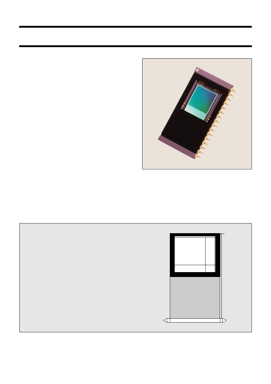
The FT 18 is a monochrome progressive-scan frame-transfer image
sensor offering 1K x 1K pixels at 30 frames per second through a
single output buffer. The combination of high speed and a high linear
dynamic range (>10 true bits at room temperature without cooling)
makes this device the perfect solution for high-end real time medical
X-ray, scientific and industrial applications. A second output can be
used for mirrored images. The device structure is shown in figure 1.
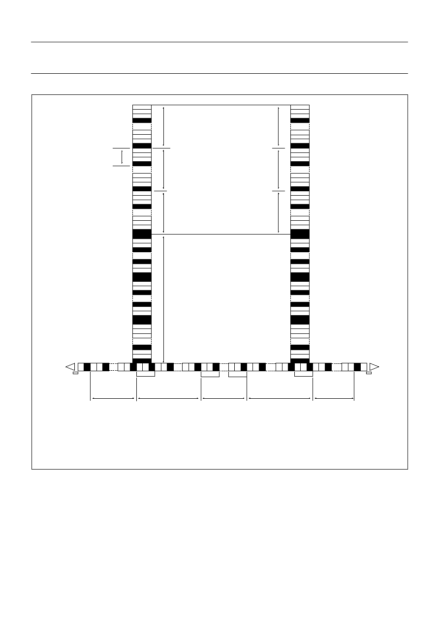
Device structure
Optical size:
7.68 mm (H) x 7.68 mm (V)
Chip size:
8.9 mm (H) x 17.0 mm (V)
Pixel size:
7.5 µm x 7.5 µm
Active pixels:
1024 (H) x 1024 (V)
Total no. of pixels:
1072 (H) x 1048 (V)
Optical black pixels:
Left: 20
Right: 20
Timing pixels:
Left: 4
Right: 4
Dummy register cells:
Left: 7
Right: 7
Contour lines:
Bottom: 1
Top: 4
Optical black lines:
Bottom: 11
Top: 8
Figure 1 - Device structure
2000 January
2
Philips Semiconductors
Product specification
Frame Transfer CCD Image Sensor
FT 18
Image
Section
1024 active pixels
1024
active
lines
20
pix
8 black line
s
2096
lines
4 contour lines
7
7
1072 cells
Output
amplifier
Output register
Storage
Section
4
20
pix
8 black lines
1 contour line
11 black lines

2000 January
3
Philips Semiconductors
Product specification
Frame Transfer CCD Image Sensor
FT 18
Architecture of the FT 18
The FT18 consists of a shielded storage section and an open image
section. Both sections have the same structure with identical cells
and properties. The only difference between the two sections is the
optical light shield.
The optical centres of all pixels in the image section form a square
grid. The charge is generated and integrated in this section. The
image section is controlled by four image clocks (A1 to A4). After
integration, the image charge is completely shifted to the storage
section. The integration time is electronically controlled by charge
reset (CR).
The storage section is controlled by four storage clocks (B1 to B4).
An output register is located below the storage section for read-out.
The output register has buffers at both ends. This allows either normal
or mirrored read-out.
Transport of the pixels in the output register is controlled by three
register clock phases (C1 to C3). The register can be used for vertical
binning. Horizontal binning can be achieved by summing pixel
charges under the floating diffusion. More information can be found
in the application note. Figure 2 shows the detailed internal structure.
IMAGE SECTION
Image diagonal
Aspect ratio
Active image width x height
Total width x height
Pixel width x height
Geometric fill factor
Image clock pins
Capacity of each clock phase
Number of active lines
Number of contour lines
Number of black lines
Total number of lines
Number of active pixels per line
Number of overscan (timing) pixels per line
Number of black reference pixels per line
Total number of pixels per line
10.9 mm
1:1
7.680 x 7.680 mm
2
8.040 x 7.860 mm
2
7.5 x 7.5 µm
2
100%
A1, A2, A3, A4
<3.75nF per pin
1024
4 (top) + 1 (bottom)
8 (top) + 11 (bottom)
1048
1024
8 (2x4)
40 (2x20)
1072
STORAGE SECTION
Storage width x height
Cell width x height
Storage clock phases
Capacity of each B phase
Number of cells per line x number of lines
8.040 x 7.860 mm
2
7.5 x 7.5 µm
2
B1, B2, B3, B4
<4.1nF per pin
1072 x 1048
OUTPUT REGISTER
Output buffers (three-stage source follower)
Number of registers
Number of register cells below storage
Number of extra cells to output
Output register horizontal transport clock pins
Capacity of each C-clock phase
Overlap capacity between neighbouring C-clocks
Reset Gate clock phases
Capacity of each RG
2
1 (bidirectional below storage)
1072
2 x 7
3 (C1..C3)
<85pF per pin
<35pF
2 pins (RGL, RGR)
<15pF
2000 January
4
Philips Semiconductors
Product specification
Frame Transfer CCD Image Sensor
FT 18
Figure 2 - Detailed internal structure
A1, A2, A3, A4: clocks of image section
B1, B2, B3, B4: clocks of storage section
C1, C2, C3: clocks of horizontal register
OG: output gate
OG
C1
OG
B4
B1
B3
A1
B3
B4
B1
A1
B3
B4
B1
A1
B3
B3
B4
B1
A1
B3
B4
A1
B4
B1
A1
A1
B3
C1
C1
C2
C2
C2
C1
C2
C1
C2
C1
1048 storage lines
C2
C1
C2
C1
C2
C2
C1
C1
C2
C1
C2
C1
C2
STORAGE
OUTR
C1
column
1
column
24+1
column
24+1K
column
24+1K+24
OUTL
One Pixel
A4
A1
A3
A3
A4
A1
A2
A3
A4
A1
A1
A3
A4
A1
A2
A3
A4
A4
A1
A2
A3
12 lines
1K active
images
lines
IMAGE
FT CCD
A2
A2
A2
A4
A1
A3
A3
A4
A1
A2
A3
A4
A1
A1
A3
A4
A1
A2
A3
A4
A4
A1
A2
A3
A2
A2
A2
12 lines
1K image pixels
7 extra cells
20 black & 4 timing columns
4 timing & 20 black columns
7 extra cells
B2
B2
B2
B2
B2
B2
B4
B1
B3
B3
B4
B1
B3
B4
B1
B3
B3
B4
B1
B3
B4
B4
B1
B3
B2
B2
B2
B2
B2
B2
C3
C3
C3
C3
C3
C3
C3
C3
C3
C3
C3
C3
C3

2000 January
5
Philips Semiconductors
Product specification
Frame Transfer CCD Image Sensor
FT 18
Specifications
1
All voltages in relation to SFS.
2
To set the VNS voltage for optimal Vertical Anti-Blooming (VAB), it should be adjustable between minimum and maximum values.
3
Guaranteed charge reset requires the CR voltage to last at least 1.2µs.
DC Conditions
1
Min.
Typical
Max.
Unit
VNS
2
VPS
SFD
SFS
VCS
OG
RD
N substrate
P substrate
Source Follower Drain
Source Follower Source
Current Source
Output Gate
Reset Drain
16
2
18
-
-2
3
12
adjusted
4
20
0
0
5.4
13
24
6
22
-
3
8
15
V
V
V
V
V
V
V
AC Clock Level Conditions
1
Min.
Typical
Max.
Unit
IMAGE CLOCKS:
A-clock swing
A-clock low level
Charge Reset (CR) level on A-clocks
3
Charge Pump (CP) level on A- clocks
9.5
-
-
-
10
0
-5
0
-
-
-
-
V
V
V
V
STORAGE CLOCKS (duty cycle=5/8):
B-clock swing
B-clock low level
9.5
-
10
0
-
-
V
V
OUTPUT REGISTER CLOCKS (duty cycle=1/2):
C-clock swing
C-clock low level
-
-
5
3
-
-
V
V
OTHER CLOCKS:
Reset Gate (RG) swing
Reset Gate (RG) low level
-
-
10
1
12
-
V
V
Absolute Maximum Ratings
Min.
Max.
Unit
GENERAL:
storage temperature
ambient temperature during operation
voltage between any two gates
DC current through any clock (absolute value)
OUT current (no short circuit protections)
-55
-40
-20
-0.2
0
+80
+60
+20
+0.2
6
°C
°C
V
µA
mA
VOLTAGES IN RELATION TO VNS:
VPS, SFS
SFD
RD
All other pins
-30
-8
-15
-32
+0.5
+8
+0.5
+0.5
V
V
V
V
VOLTAGES IN RELATION TO VPS:
VNS
SFD, RD
SFS
All other pins
-0.5
+0
-8
-20
+30
+30
+8
+20
V
V
V
V
2000 January
6
Philips Semiconductors
Product specification
Frame Transfer CCD Image Sensor
FT 18
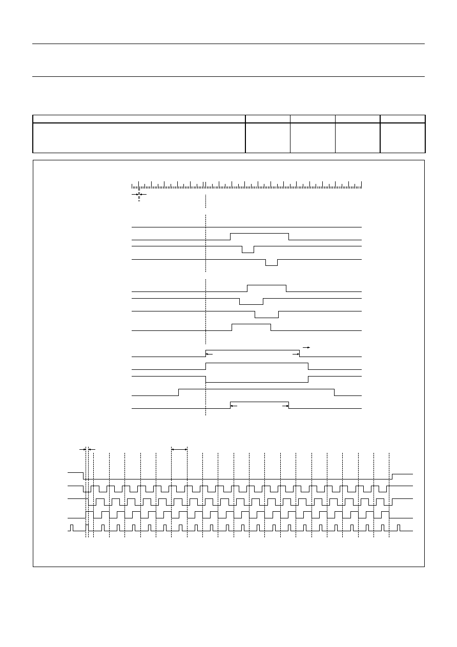
Timing diagrams (for default operation)
Figure 3 - Line and pixel timing diagrams
H
L
SSC
H
L
H
L
H
L
C1
C2
C3
Tp/6 = (1/36MHz)/6 = 4.63ns
dummy 1
. . . . . . .
dummy 7
black 1
. . . . . . .
black 20
timing 1
timing 4
pixel 1
. . . . . . .
pixel 1024
timing 1
timing 4
black 1
. . . . . . .
black 20
dummy 1
H
L
RG
Tp = 1/36MHz = 27.8ns
. . . . . . .
. . . . . . .
In this figure, charge is transported to the left output buffer (normal readout) by moving it from C1 to C2 to C3 etc.
By exchanging the timing of C1 and C2, charge will be transported to the right output buffer (mirrored readout).
A1
A2
A3
A4
Phase
or
pixel count
1100 1110 1120 1130 1140
10
20
30
40
50
60
70
80
90
100
110
120
L
H
L
H
L
H
L
H
B2
B3
B4
B1
L
H
L
H
L
H
L
H
19
64
28
37
46
55
32
62
26
44
38
56
20
50
SSC
L
H
72
1150
0
0
One cycle of the storage gates (during line blanking), moving one line from storage to output register
C clocks stopped for 2 microseconds
L
H
PB
0
L
H
BLC
0
79
79
L
H
CB
1131
99
1080 pixels until 1152
1/(36MHz) = 27.8ns
One charge pumping cycle of the image gates (during line blanking), shifting the charge of one line back and forth
Start-Stop C-clocks
Pre-Blanking
Black Level Clamp
Composite Blanking
L
CR
19
64
Charge Reset
H
1.25 microseconds
AC Characteristics
Min.
Typical
Max.
Unit
Horizontal frequency (1/Tp)
Vertical frequency
-
-
36
750
40
833
MHz
kHz
Line Timing
Pixel Timing
2000 January
7
Philips Semiconductors
Product specification
Frame Transfer CCD Image Sensor
FT 18
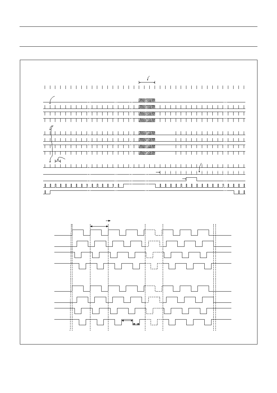
Figure 4 - Frame timing diagrams
Frame Timing
Frame Shift Timing
A1
L
H
Tp=1/(36MHz) = 27.8ns
A2
L
H
A3
L
H
A4
L
H
1
2
1048
1047
B1
L
H
B2
L
H
B3
L
H
B4
L
H
1
2
1048
1047
48 Tp 750kHz
18Tp
30Tp
for all A and B clocks,
duty cycle = 5/8
1109 1110 1111 1112 1113 1114 1115 1116
1119 1120 1121 1122
...... 1250
1
......
26
27
......
70
71
72
73
74
75
76
77
78
79
80
81
82
83
86
87
1024 D
D
B
B
BLC BLC
B
B
D
D
E
internal
LINE
counter
E
E
E
E
B
B
BLC BLC
B
B
D
D
C
C
1
video
line no.
A1
A2
A3
A4
L
H
L
H
L
H
L
H
B1
B2
B3
B4
L
H
L
H
L
H
L
H
CR
BLC
SSC
PB
L
H
L
H
L
H
L
H
By adding one CR-pulse during the horizontal blanking,
the effective integration time is decreased: "electronic shuttering"
CB
L
H
CR before nominal integration
......
......
88
2
charge image (all lines) is moved from image to storage
by the image and storage clocks together (see Figure "Frame Shift Timing").
Frame Transfer (FT):
Charge Pump (CP): a measure to reduce dark current due to interface states.
For details see figure 3 "Line and pixel timing diagrams".
Hustle: moving the charge packets of one line from storage to the output register.
For details see figure 3 "Line and pixel timing diagrams".
Linetime: the C-clocks shift charge packets one-by-one to the selected output buffer.
For details see figure 3 "Line and pixel timing diagrams".
Black-Level Clamp (BLC): the video processing clamps the black lines to determine its output zero-level.

2000 January
8
Philips Semiconductors
Product specification
Frame Transfer CCD Image Sensor
FT 18
Performance
The performance of the FT 18 is described for modes of operation
with 25 frames/sec or 30 frames/sec respectively. Measurements
for the FT 18 are done under the following circumstances (values in
brackets apply for the 30 frames/sec mode):
· VNS is adjusted as low as possible while maintaining proper
Vertical Anti-Blooming.
· Integration takes place under 2 gates with 10V clock swing during
40ms (33.33ms)
· The vertical transport or frame shift frequency equals 750kHz
(714kHz).
· The horizontal transport or read-out frequency equals 36MHz
(40MHz).
· The RMS read-out noise of the output buffers and the FPN are
measured in the bandwidth 0.1-18MHz (0.1-20MHz).
· The performance in dark is given at a temperature of 318K / 45°C.
Note that the dark current decreases by a factor of two for every
decrease of temperature of approximately 10°C.
1
White Shading is defined as the ratio of the one-
value of an 8x8 pixel blurred image (low-pass) to the mean signal value.
2
Random Non Uniformity is defined as the ratio of the one-
value of the highpass image to the mean signal value at nominal light.
3
Q
max
is determined from the lowpass filtered image.
4
Q
max
of the output register may be increased up to 200kel. In this case the charge packets of the pixels may get mixed in the output register
during horizontal transport. This may reduce the number of times that the output register needs to be read out if lines are read out solely to be
dumped.
5
The smear condition is: overexposure with a spot with a height of 10% of the image height (approx. 100 lines).
Linear / Saturation
Min.
Typical
Max.
Unit
Overexposure over entire area while maintaining good VAB
Vertical resolution (MTF) @ 67 lp/mm
Quantum efficiency @ 450 nm
Quantum efficiency @ 520 nm
Quantum efficiency @ 600 nm
Quantum efficiency @ 800 nm (near IR)
Image lag
White Shading
1
Random Non-Uniformity (RNU)
2
Full-well capacity Floating Diffusion (FD)
Full-well capacity saturation level (Q
max
)
3
image
Full-well capacity saturation level (Q
max
) storage
Full-well capacity saturation level (Q
max
) output register
4
300
25
10
21
18
5
-
-
-
120
40
45
90
-
-
11
22
19
-
0
-
1.0
-
45
-
-
-
-
-
-
-
-
-
2.5
1.4
-
-
-
-
lux
%
%
%
%
%
%
%
%
kel.
kel.
kel.
kel.
25 frames/sec mode only
Sensitivity @ 3200K without IR cut-off filter
Smear without shutter
5
Dynamic range
RMS read-out noise
5.6
-
60
-
5.8
-
63.8
29
-
0.39
-
38
kel/lux
%
dB
el
30 frames/sec mode only
Sensitivity @ 3200K without IR cut-off filter
Smear without shutter
5
Dynamic range
RMS read-out noise
4.6
-
60
-
4.8
-
63.5
30
-
0.40
-
40
kel/lux
%
dB
el
2000 January
9
Philips Semiconductors
Product specification
Frame Transfer CCD Image Sensor
FT 18
Figure 5 - Quantum efficiency versus wavelength
Quantum efficiency (%)
Wavelength (nm)
400
500
600
700
800
900
30
20
10
0

2000 January
10
Philips Semiconductors
Product specification
Frame Transfer CCD Image Sensor
FT 18
1
Black level offset is defined as the difference in dark signal of a black refence line and an active image line.
2
FPN is the one-
value of the highpass image.
Dark Condition
Min.
Typical
Max.
Unit
Dark current
Black level offset
1
-
-
-
-
240
25
pA/cm
2
el
Dark condition at 25 frames/sec:
Average dark signal
Shot noise of the dark current
Horizontal shading
Vertical shading
Fixed Pattern Noise
2
in dark (FPN)
-
-
-
-
-
56
-
-
-
-
67
10
25
66
19
el
el
el
el
el
Dark condition at 30 frames/sec:
Average dark signal
Shot noise of the dark current
Horizontal shading
Vertical shading
Fixed Pattern Noise
2
in dark (FPN)
-
-
-
-
-
47
-
-
-
-
56
10
25
56
19
el
el
el
el
el
Output Buffers
Min.
Typical
Max.
Unit
Conversion factor
Supply current
Bandwidth
Output impedance buffer (R
load
= 3.3k
, C
load
= 2pF)
8.5
10
4
110
400
11.5
µV/el.
mA
MHz

2000 January
11
Philips Semiconductors
Product specification
Frame Transfer CCD Image Sensor
FT 18
Application information
Current handling
One of the purposes of VPS is to drain the holes that are generated
during exposure of the sensor to light. Free electrons are either
transported to the VRD connection and, if excessive (from over-
exposure), free electrons are drained to VNS. No current should
flow into any VPS connection of the sensor. During high overexposure
a total current 10 to 15mA through all VPS connections together
may be expected. The PNP emitter follower in the circuit diagram
(figure 6) serves these current requirements.
VNS drains superfluous electrons as a result of overexposure. In
other words, it only sinks current. During high overexposure a total
current of 10 to 15mA through all VNS connections together may be
expected. The NPN emitter follower in the circuit diagram meets
these current requirements.
Decoupling of DC voltages
All DC voltages should be decoupled with a 100nF decoupling
capacitor. This capacitor must be mounted as close as possible to
the sensor pin. Further noise reduction (by bandwidth limiting) is
achieved by the resistors in the connections between the sensor
and its voltage supplies. The electrons that build up the charge
packets that will reach the floating diffusions only add up to a small
current, which will flow through VRD. Therefore a large series resistor
in the VRD connection may be used.
Outputs
To limit the on-chip power dissipation, the output buffers are designed
with open source outputs. Outputs to be used should therefore be
loaded with a current source or more simply with a resistance to
GND. In order to prevent the output (which typically has an output
impedance of about 400
) from bandwidth limitation as a result of
capacitive loading, load the output with an emitter follower built from
a high-frequency transistor. Mount the base of this transistor as close
as possible to the sensor and keep the connection between the
emitter and the next stage short. The CCD output buffer can easily
be destroyed by ESD. By using this emitter follower, this danger is
suppressed; do NOT reintroduce this danger by measuring directly
on the output pin of the sensor with an oscilloscope probe. Instead,
measure on the output of the emitter follower. Slew rate limitation is
prevented by avoiding a too-small quiescent current in the emitter
follower; about 10mA should do the job. The collector of the emitter
follower should be decoupled properly to suppress the Miller effect
from the base-collector capacitance.
A CCD output load resistor of 3.3k
typically results in a bandwidth
of 110MHz. The bandwidth can be enlarged to about 130MHz by
using a resistor of 2.2k
instead, which, however, also enlarges the
on-chip power dissipation.
Device protection
The output buffers of the FT 18 are likely to be damaged if VPS
rises above SFD or RD at any time. This danger is most realistic
during power-on or power-off of the camera. The RD voltage should
always be lower than the SFD voltage.
Never exceed the maximum output current. This may damage the
device permanently. The maximum output current should be limited
to 6mA.
Be especially aware that the output buffers of these image sensors
are very sensitive to ESD damage.
Because of the fact that our CCDs are built on an n-type substrate,
we are dealing with some parasitic npn transistors. To avoid activation
of these transistors during switch-on and switch-off of the camera,
we recommend the application diagram of figure 6.
2000 January
12
Philips Semiconductors
Product specification
Frame Transfer CCD Image Sensor
FT 18
Figure 6 - Application diagram to protect the FT 18
Device Handling
An image sensor is a MOS device which can be destroyed by electro-
static discharge (ESD). Therefore, the device should be handled
with care.
Always store the device with short-circuiting clamps or on conductive
foam. Always switch off all electric signals when inserting or removing
the sensor into or from a camera (the ESD protection in the CCD
image sensor process is less effective than the ESD protection of
standard CMOS circuits).
Being a high quality optical device, it is important that the cover
glass remain undamaged. When handling the sensor, use fingercots.
When cleaning the glass we recommend using ethanol (or possibly
water). Use of other liquids is strongly discouraged:
· if the cleaning liquid evaporates too quickly, rubbing is likely to
cause ESD damage.
· the cover glass and its coating can be damaged by other liquids.
Rub the window carefully and slowly.
Dry rubbing of the window may cause electro-static charges or
scratches which can destroy the device.
BAT74
Schottky!
VPS
SFD
VRD
BC
860C
BC
850C
VNS
100nF
100nF
100nF
BC
850C
0.5-1mA
27
15
10k
0.5-1mA
VCS
VOG
10k
10k
OUT
<7pF!
keep short
<10mm!
keep short!
output for
preprocessing
BFR
92A
1k
3.3k
10mA
100nF
100nF
100nF
BAT74
0.5-1mA
BAT74
Schottky!
100
VSFD
100nF

2000 January
13
Philips Semiconductors
Product specification
Frame Transfer CCD Image Sensor
FT 18
Pin configuration
The FT18 is mounted in a ceramic DIL 32-pin package.
The position of pin 1 is marked with a white dot on top of the package.
Pinning
Symbol
Name
Pin #
VNS
VNS
VPS
VPS
SFDL
SFDR
SFSL
SFSR
VCSL
VCSR
OGL
OGR
RDL
RDR
A1
A2
A3
A4
B1
B2
B3
B4
C1
C1
C2
C2
C3
C3
RGL
RGR
OUTL
OUTR
N substrate
N substrate
P well
P well
Source Follower Drain Left
Source Follower Drain Right
Source Follower Source Left
Source Follower Source Right
Current Source Gate Left
Current Source Gate Right
Output Gate left
Output Gate Right
Reset Drain Left
Reset Drain Right
Image Clock (Phase 1)
Image Clock (Phase 2)
Image Clock (Phase 3)
Image Clock (Phase 4)
Storage Clock (Phase 1)
Storage Clock (Phase 2)
Storage Clock (Phase 3)
Storage Clock (Phase 4)
Register Clock (Phase 1)
Register Clock (Phase 1)
Register Clock (Phase 2)
Register Clock (Phase 2)
Register Clock (Phase 3)
Register Clock (Phase 3)
Reset Gate Left
Reset Gate Right
Output Left
Output Right
12
21
5
28
9
24
8
25
7
26
6
27
11
22
3
4
30
29
1
2
32
31
14
19
15
18
16
17
13
20
10
23
2000 January
14
Philips Semiconductors
Product specification
Frame Transfer CCD Image Sensor
FT 18
Figure 7 - FT18 pin configuration (top view)
C2
B4
B2
VPS
B1
B3
SFDR
VCSL
SFSR
RGL
C3
OGL
RDL
OUTL
C1
VNS
VNS
1
2
3
4
5
6
7
8
9
10
11
12
13
14
15
16
32
31
30
29
28
27
26
25
24
23
22
21
20
19
18
17
VPS
SFSL
VCSR
OGR
RDR
A2
A1
A4
A3
C1
C2
C3
RGR
OUTR
SFDL
B4
B1
B4
B1
IMAGE
TOP
FT18
STORAGE
2000 January
15
Philips Semiconductors
Product specification
Frame Transfer CCD Image Sensor
FT 18
Package information
Figure 8 - Mechanical drawing of the FT 18 package
Angle of rotation: less than ± 1
0
Sensor flatness: < 7 µm (P-V)
Cover glass: Corning 7059
Thickness of cover glass: 0.8 ± 0.05
Refractive index: n
d
= 1.53
Single sided AR coating inside, 21% reflection (430-660 nm)
All drawing units are in mm.
15.494 ±0.25
7.747 ±0.2
3.317 ±0.2
15.24 ±0.25
15 ±0.1
Sensor crystal
Cover glass
Anti-reflex
coating
0.25 +0.05 -0.02
29.70 ±0.3
9.575 ±0.2
4.92 ±0.2
7.68 ±0.2
25.4 ±0.1
0.78 ±0.05
0.48 ±0.05
1.778 ±0.13
4.5 ±0.3
3.3 ±0.2
0.762 ±0.07
2.868 ±0.29
1.090 ±0.11
2.986 ±0.29
0.665 ±0.07
0.8 ±0.05
0.08 +0.07 -0.02
Glue
0.725 ±0.05
Crystal + Glue
1.016 ±0.10
1.4 / 100
1 / 100
B
B
0.005
Image area

Order codes
The sensor can be ordered using the following code:
You can contact the Image Sensors division of Philips
Semiconductors at the following address:
Philips Semiconductors
Image Sensors
Internal Postbox WAG-05
Prof. Holstlaan 4
5656 AA Eindhoven
The Netherlands
phone
+31 - 40 - 27 44 400
fax
+31 - 40 - 27 44 090
www.semiconductors.philips.com/imagers/
Philips reser
v
es the r
ight to change an
y inf
o
r
mation contained herein without notice
.
All inf
o
r
mation fur
nished b
y
Philips is b
elie
v
ed to be accur
ate
.
© Philips Electronics N.V
.
2000
9922 157 32001
Philips
Semiconductors
Philips Semiconductors
Product specification
Frame Transfer CCD Image Sensor
FT 18
TRAD
lmtb
FT18 sensors
Description
Quality Grade
Order Code
FT18/TG
FT18/IG
FT18/HG
FT18/SG
Test grade
Industrial grade
High grade
Selected grade
9922 157 32031
9922 157 32021
9922 157 32011
9922 157 32001
Document Outline
- Description
- Device structure
- Architecture of the FT 18
- Specifications
- Timing diagrams (for default operation)
- Performance
- Application information
- Device Handling
- Pin configuration
- Package information
- Order codes