Frame Transfer CCD Image Sensor

FTT1010-M
Frame Transfer CCD Image Sensor
Philips
Semiconductors
IMAGE SENSORS
Product specification
1999 September 21
File under Image Sensors
TRAD
1999 September
2
Philips Semiconductors
Product specification
Frame Transfer CCD Image Sensor
FTT1010-M
·
1-inch optical format
·
1M active pixels (1024H x 1024V)
·
Progressive scan
·
Excellent anti-blooming
·
Variable electronic shuttering
·
Square pixel structure
·
H and V binning
·
100% optical fill factor
·
High dynamic range (>72dB)
·
High sensitivity
·
Low dark current and fixed pattern noise
·
Low read-out noise
·
Data rate up to 2 x 40 MHz
·
Mirrored and split read-out
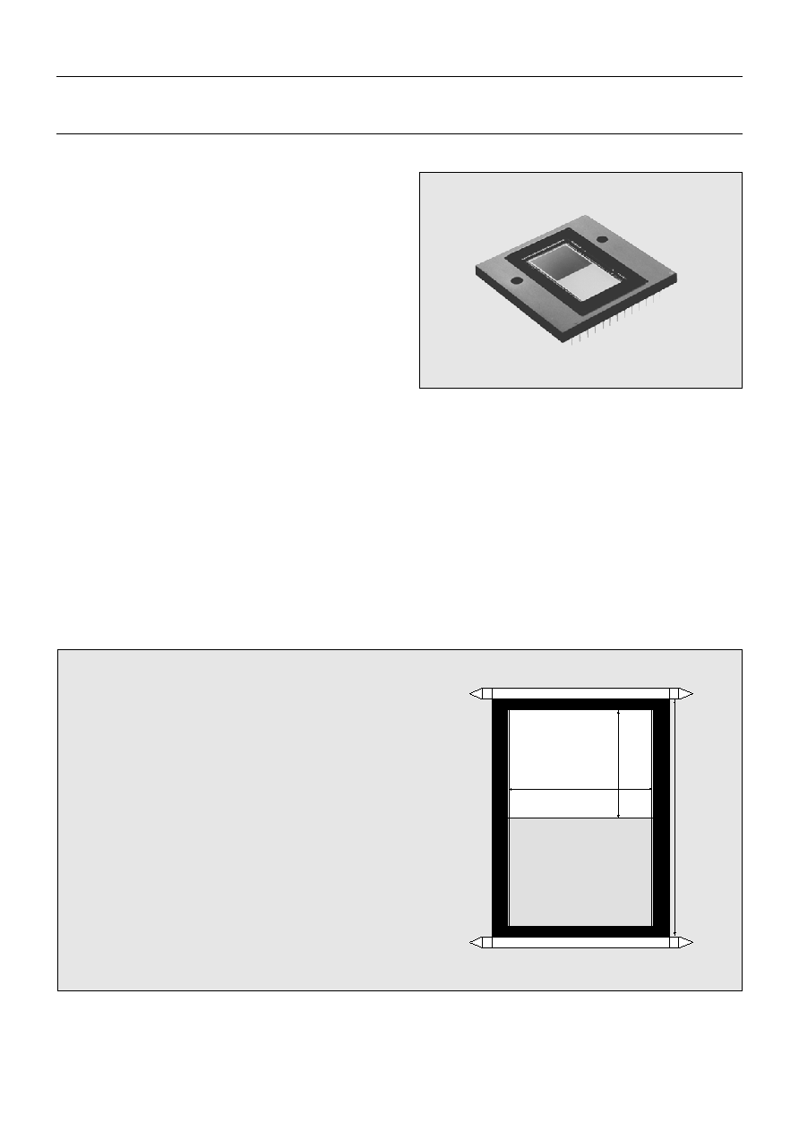
Description
The FTT 1010-M is a monochrome progressive-scan frame-transfer
image sensor offering 1K x 1K pixels at 30 frames per second through
a single output buffer. The combination of high speed and a high
linear dynamic range (>12 true bits at room temperature without
cooling) makes this device the perfect solution for high-end real time
medical X-ray, scientific and industrial applications. A second output
can either be used for mirrored images, or can be read out
simultaneously with the other output to double the frame rate. The
device structure is shown in figure 1.
Device structure
Optical size:
12.288 mm (H) x 12.288 mm (V)
Chip size:
14.572 mm (H) x 26.508 mm (V)
Pixel size:
12 µm x 12 µm
Active pixels:
1024 (H) x 1024 (V)
Total no. of pixels:
1072 (H) x 1030 (V)
Optical black pixels:
Left: 20
Right: 20
Timing pixels:
Left: 4
Right: 4
Dummy register cells:
Left: 7
Right: 7
Optical black lines:
Bottom: 6 Top: 6
Figure 1 - Device structure
Image Section
1024 active pixels
1024
active
lines
20
6 black lines
6 black lines
2060
lines
4
7
7
1072 cells
Output
amplifier
Output register
Storage Section
20
4
Z
Y
W
X

1999 September
3
Philips Semiconductors
Product specification
Frame Transfer CCD Image Sensor
FTT1010-M
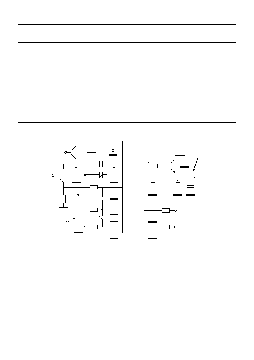
Architecture of the FTT1010-M
The FTT1010-M consists of a shielded storage section and an open
image section. Both sections are electronically the same and have
the same cell structure with the same properties. The only difference
between the two sections is the optical light shield.
The optical centres of all pixels in the image section form a square
grid. The charge is generated and integrated in this section. Output
registers are located below the storage section. The output amplifiers
Y and Z are not used in Frame Transfer mode and should be
connected as not-used amplifiers.
After the integration time the charge collected in the image section
is shifted to the storage section. The charge is read out line by line
through the lower output register.
The left and the right half of each output register can be controlled
independently. This enables either single or multiple read-out.
During vertical transport the C3 gates separate the pixels in the
register. The letters W, X, Y and Z are used to define the four
quadrants of the sensor. The central C3 gates of both registers are
part of the W and Z quadrants of the sensor.
Both upper and lower registers can be used for vertical binning.
Both registers also have a summing gate at each end that can be
used for horizontal binning. Figure 2 shows the detailed internal
structure.
OUTPUT REGISTERS
Output buffers (three-stage source follower)
Number of registers
Number of dummy cells per register
Number of register cells per register
Output register horizontal transport clock pins
Capacity of each C-clock phase
Overlap capacity between neighbouring C-clocks
Output register Summing Gates
Capacity of each SG
Reset Gate clock phases
Capacity of each RG
4 (one on each corner)
2 (one above, one below)
14 (2x7)
1072
C1, C2, C3
60pF per pin
20pF
4 pins (SG)
15pF
4 pins (RG)
15pF
IMAGE SECTION
Image diagonal (active video only)
Aspect ratio
Active image width x height
Pixel width x height
Geometric fill factor
Image clock pins
Capacity of each clock phase
Number of active lines
Number of black reference lines
Number of dummy black lines
Total number of lines
Number of active pixels per line
Number of overscan (timing) pixels per line
Number of black reference pixels per line
Total number of pixels per line
17.38 mm
1:1
12.288 x 12.288 mm
2
12x12 µm
2
100%
A1, A2, A3, A4
2.5nF per pin
1024
2
4
1030
1024
8 (2x4)
40 (2x20)
1072
STORAGE SECTION
Storage width x height
Cell width x height
Storage clock phases
Capacity of each clock phase
Number of cells per line
Number of lines
12.864 x 12.360 mm
2
12x12 µm
2
B1, B2, B3, B4
2.5nF per pin
1072
1030
1999 September
4
Philips Semiconductors
Product specification
Frame Transfer CCD Image Sensor
FTT1010-M
Figure 2 - Detailed internal structure
SG: summing gate
OG: output gate
RG: reset gate
RD: reset drain
A1, A2, A3, A4: clocks of image section
B1, B2, B3, B4: clocks of storage section
C1, C2, C3: clocks of horizontal registers
One Pixel
A3
A4
A2
A3
A4
A2
A1
A2
A3
A4
A2
A3
A4
A1
A2
A3
A4
A2
A3
A4
A1
B2
B3
RG
A1
B2
B3
A3
A3
A4
B4
A2
A1
B2
B3
B3
B4
B4
B2
A1
B2
B3
B3
B4
B4
B2
B4
B3
B2
B4
B3
B2
A4
B4
A3
A2
OUT_Z
RD
OUT_Y
6 black
lines
20 black & 4
timing columns
1K image
20 black & 4 timing
columns
7 dummy
pixels
C1
C1
SG C2
OG
C2
C2
C1
C2
C1
C2
C1
C2
C1
C2
C2
C1
C1
C2
C1
C2
C1
C2
C1
C2
C1
SG OG
C1
C3
C1
C1
C2
C2
C2
C1
C2
C1
C2
C1
C3
1K active
images lines
column
1
column
24 + 1K + 24
C1
C2
C2
C1
column
24 + 1
column
24 + 1K
C2 C1
C1
C2
RD
RG
RG
7 dummy
pixels
SG
OG
OUT_W
RG
RD
OUT_X
RG
RD
C1
SG OG
STORAGE
FT CCD
IMAGE
1K storage
lines
6 black lines
C2
C1
C2
C2
C1
C1
A1
A1
A1
(not used)
(not used)
pixels
C3
A1
B1
B1
B1
B1
B1
B1
B1
B1
B1
B1
C3
C3
C3
C3
C3
C3
C3
C3
C3
C3
C3
C3
C3
C3
C3
C3
C3
C3
C3
C3
C3
C3

1999 September
5
Philips Semiconductors
Product specification
Frame Transfer CCD Image Sensor
FTT1010-M
Specifications
1
During Charge Reset it is allowed to exceed maximum rating levels (see note
5
).
2
All voltages in relation to SFS.
3
To set the VNS voltage for optimal Vertical Anti-Blooming (VAB), it should be adjustable between minimum and maximum values.
4
Three-level clock is preferred for maximum charge; the swing during vertical transport should be 4V higher than the voltage during integration.
A two level clock (typically 10V) can be used if a lower maximum charge handling capacity is allowed.
5
Charge Reset can be achieved in two ways:
· The typical CR level is applied to all image clocks simultaneously (preferred).
· The typical A-clock low level is applied to all image clocks; for proper CR, an additional Charge Reset pulse on VNS is required. This will also affect
the charge handling capacity in the storage areas.
DC CONDITIONS
2
MIN. [V]
TYPICAL [V]
MAX. [V]
MAX. [mA]
VNS
3
VPS
SFD
SFS
VCS
OG
RD
N substrate
P substrate
Source Follower Drain
Source Follower Source
Current Source
Output Gate
Reset Drain
18
1
16
-
-5
4
13
24
3
20
0
0
6
15.5
28
7
24
-
3
8
18
15
15
4.5
1
-
-
-
AC CLOCK LEVEL CONDITIONS
2
MIN.
TYPICAL
MAX.
UNIT
IMAGE CLOCKS:
A-clock amplitude during integration and hold
A-clock amplitude during vertical transport (duty cycle=5/8)
4
A-clock low level
Charge Reset (CR) level on A-clock
5
8
10
-5
10
14
0
-5
V
V
V
V
STORAGE CLOCKS:
B-clock amplitude during hold
B-clock amplitude during vertical transport (duty cycle=5/8)
8
10
10
14
V
V
OUTPUT REGISTER CLOCKS:
C-clock amplitude (duty cycle during hor. transport = 3/6)
C-clock low level
Summing Gate (SG) amplitude
Summing Gate (SG) low level
4.75
2
5
3.5
10
3.5
5.25
10
V
V
V
V
OTHER CLOCKS:
Reset Gate (RG) amplitude
Reset Gate (RG) low level
Charge Reset (CR) pulse on Nsub
5
5
0
10
3
10
10
10
V
V
V
ABSOLUTE MAXIMUM RATINGS
1
MIN.
MAX.
UNIT
GENERAL:
storage temperature
ambient temperature during operation
voltage between any two gates
DC current through any clock phase (absolute value)
OUT current (no short circuit protection)
-55
-40
-20
-0.2
0
+80
+60
+20
+2.0
10
°C
°C
V
µA
mA
VOLTAGES IN RELATION TO VPS:
VNS, SFD, RD
VCS, SFS
all other pins
-0.5
-8
-5
+30
+5
+25
V
V
V
VOLTAGES IN RELATION TO VNS:
SFD, RD
VCS, SFS, VPS
all other pins
-15
-30
-30
+0.5
+0.5
+0.5
V
V
V
1999 September
6
Philips Semiconductors
Product specification
Frame Transfer CCD Image Sensor
FTT1010-M
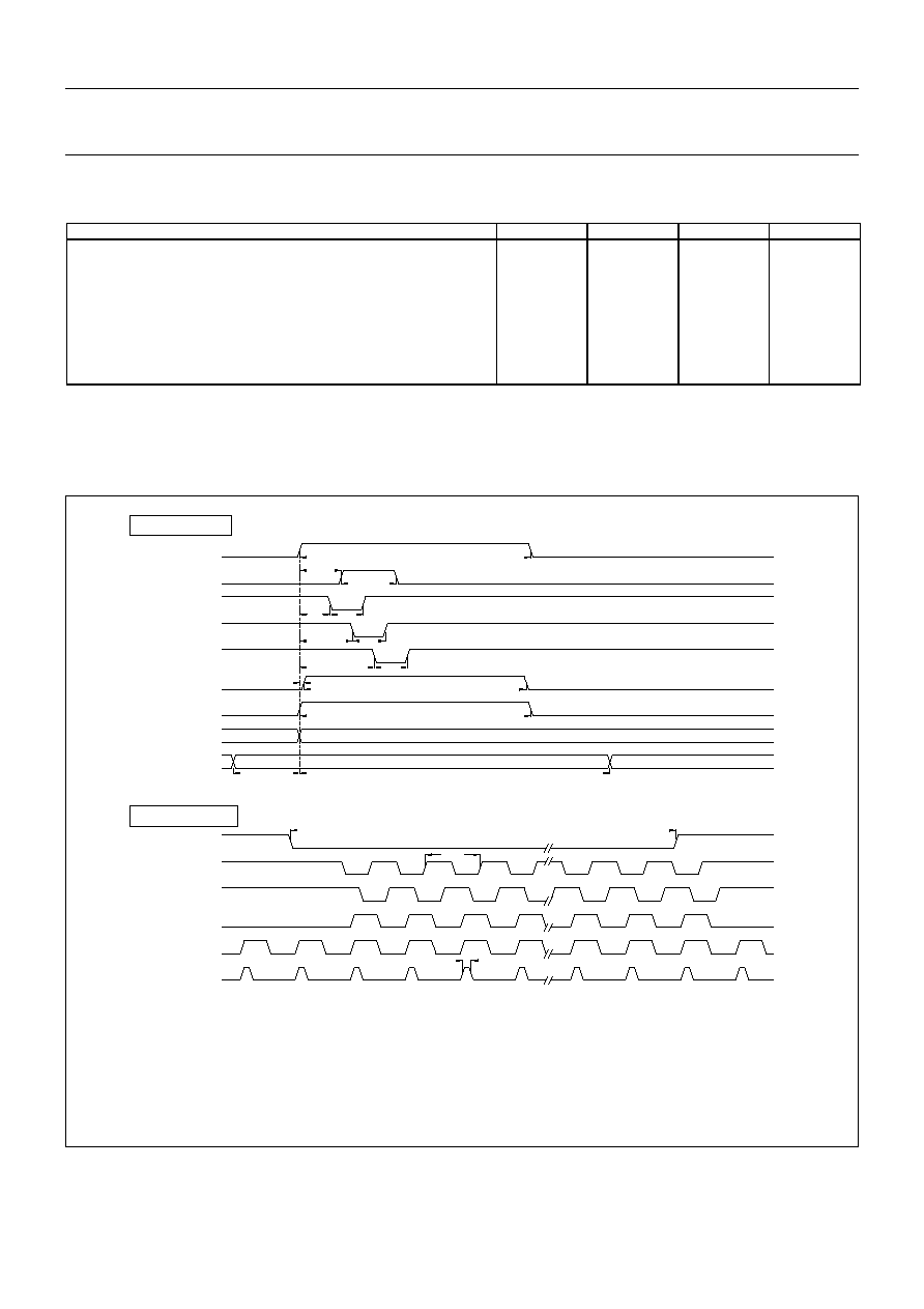
Timing diagrams (for default operation)
C1 to C3: Horizontal register clocks
SSC: Start-Stop C-clocks
SG: Summing gate
RG: Reset gate
VD: Frame pulse
CR: Charge Reset
BLC: Black Level Clamp
B1 to B4: Vertical storage clocks
1
Tp = 1 clock period
2
Duty cycle = 50% and phase shift of the C clocks is 120 degrees.
AC CHARACTERISTICS
MIN.
TYPICAL
MAX.
UNIT
Horizontal frequency (1/Tp)
1
Vertical frequency
Charge Reset (CR) time
Rise and fall times:
image clocks (A)
storage clocks (B)
register clocks (C)
2
summing gate (SG)
reset gate (RG)
0
0
2
10
10
3
3
3
18
450
5
20
20
5
5
5
40
1000
1/6 Tp
1/6 Tp
1/6 Tp
MHz
kHz
µs
ns
ns
ns
ns
ns
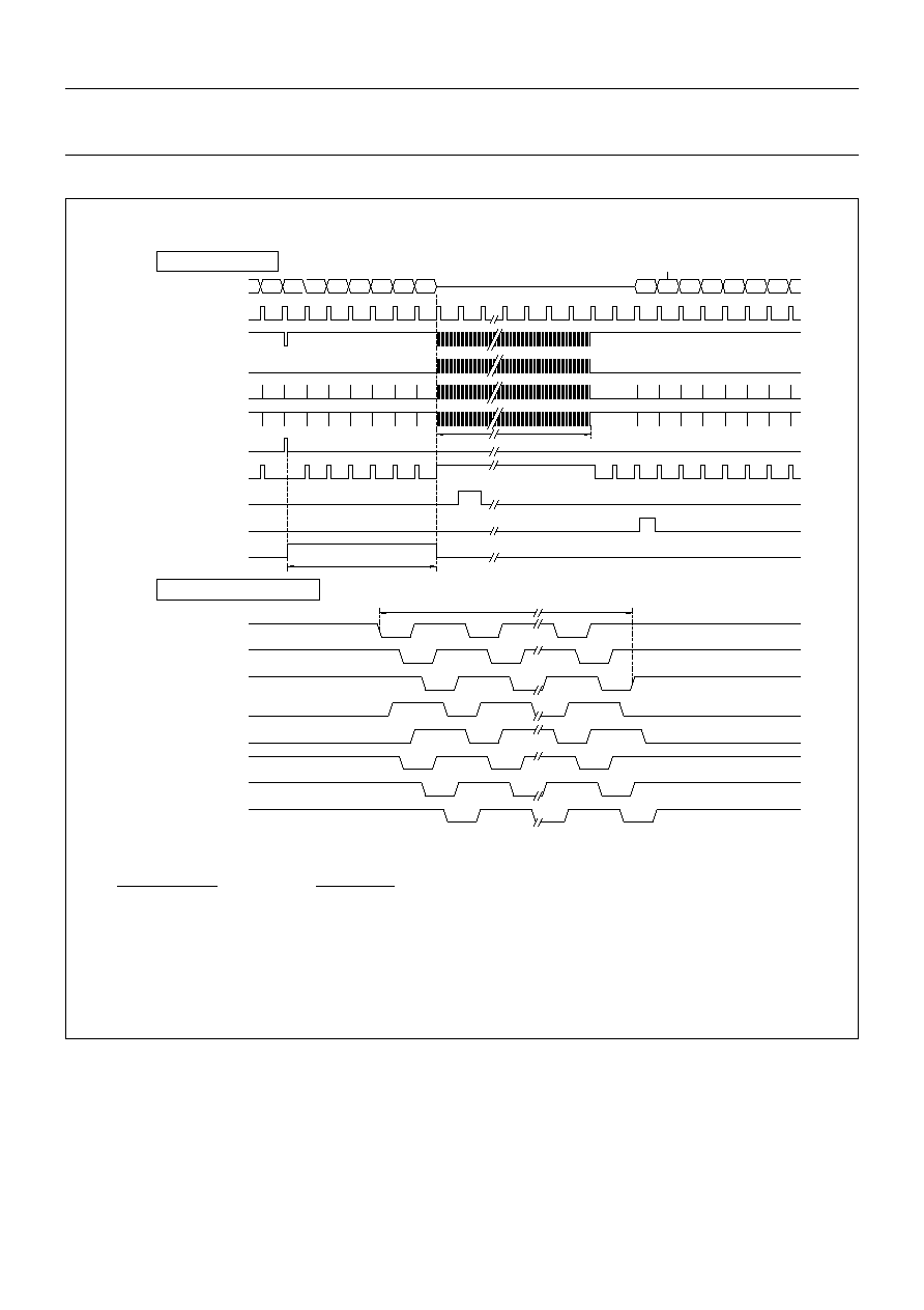
Figure 3 - Line and pixel timing diagrams
SSC
B1
B2
B3
B4
CR
AHigh
VD
BLC
C1
C2
C3
SG
RG
SSC
Tp = 1 clock period = 1 / 18MHz = 55.56ns
Pixel output sequence: 7 dummy, 20 black, 4 timing, 1024 active, 4 timing, 20 black
Line Time: 1184 x Tp = 65.7µs
Line Timing
Pixel Timing
* During AHigh = H the phiA high level is increased from 10V to 14V
*
L
L
H
H
L
H
H
L
H
L
L
L
H
H
H
L
L
H
H
L
L
H
L
H
H
H
L
L
L
H
1Tp
1079 pixels
Tp / 6
105Tp
34Tp
15Tp
15Tp
15Tp
25Tp
24Tp
14Tp
19Tp
Tp
105
Tp
101
Tp
2
141Tp
30Tp
1999 September
7
Philips Semiconductors
Product specification
Frame Transfer CCD Image Sensor
FTT1010-M
VD: Frame pulse
CR: Charge Reset
BLC: Black Level Clamp
A1 to A4: Vertical image clocks
B1 to B4: Vertical storage clocks
C1 to C3: Horizontal register clocks
SSC: Start-Stop C-clocks
SG: Summing gate
RG: Reset gate
Figure 4 - Frame timing diagrams
1
8 phases correspond with 2 line shifts
N =
,
for example:
= 5
Horizontal freq.
Vertical freq. x 8
18MHz
450kHz x 8
Sensor Output
A2
VD
BLC
A3
B
B
B
B
1
2
Integration Time
Ahigh
CR
H
L
A1
EXT. SHUTTER
Frame Timing
Black
*
Frame Shift
B2, B3, B4
A4
B
1019
1024
1023
1022
1021
1020
4
3
Tframe shift = 1027 x 8 x N clock periods
B4
B3
B2
B1
Frame Shift Timing
SSC
A1, A2, A3
A4
B1
L
H
L
H
L
H
L
H
L
H
L
H
L
H
L
H
L
H
L
L
H
H
H
L
L
L
H
H
L
H
H
L
L
H
1
1999 September
8
Philips Semiconductors
Product specification
Frame Transfer CCD Image Sensor
FTT1010-M
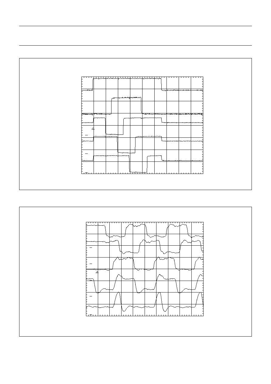
Y / Div.
: 10V (B1, B2, B3, B4); 5V (SSC)
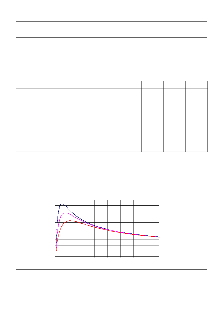
Y / Div.
: 5V (C1, C2, C3); 10V (SG, RG)
Line timing
Pixel timing
SSC
B1
B2
B3
B4
C1
C2
C3
SG
RG
Figure 6 - Start horizontal readout
Figure 5 - Vertical readout
--> time
--> time
1999 September
9
Philips Semiconductors
Product specification
Frame Transfer CCD Image Sensor
FTT1010-M
Performance
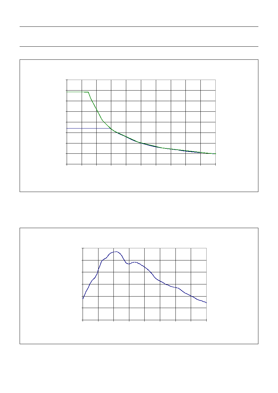
The test conditions for the performance characteristics are as follows:
· All values are measured using typical operating conditions.
· VNS is adjusted as low as possible while maintaining proper
Vertical Anti-Blooming.
· Sensor temperature = 60°C (333K).
· Horizontal transport frequency = 18MHz.
1
Linear dynamic range is defined as the ratio of Q
lin
to read-out noise (the latter reduced by Correlated Double Sampling).
2
Charge Transfer Efficiency values are tested by evaluation and expressed as the value per gate transfer.
3
Smear is defined as the ratio of 10% of the vertical transport time to the integration time. It indicates how visible a spot of 10% of the image
height would become.
4
White Shading is defined as the ratio of the one-
value of the pixel output distribution expressed as a percentage of the mean value output
(low pass image).
5
RNU is defined as the ratio of the one-
value of the highpass image to the mean signal value at nominal light.
· Vertical transport frequency = 450kHz (unless specified otherwise).
· Integration time = 10ms (unless specified otherwise).
· The light source is a 3200K lamp with neutral density filters and
a 1.7mm thick BG40 infrared cut-off filter. For Linear Operation
measurements, a temperature conversion filter (Melles Griot type
no. 03FCG261, -120 mired, thickness: 2.5mm) is applied.
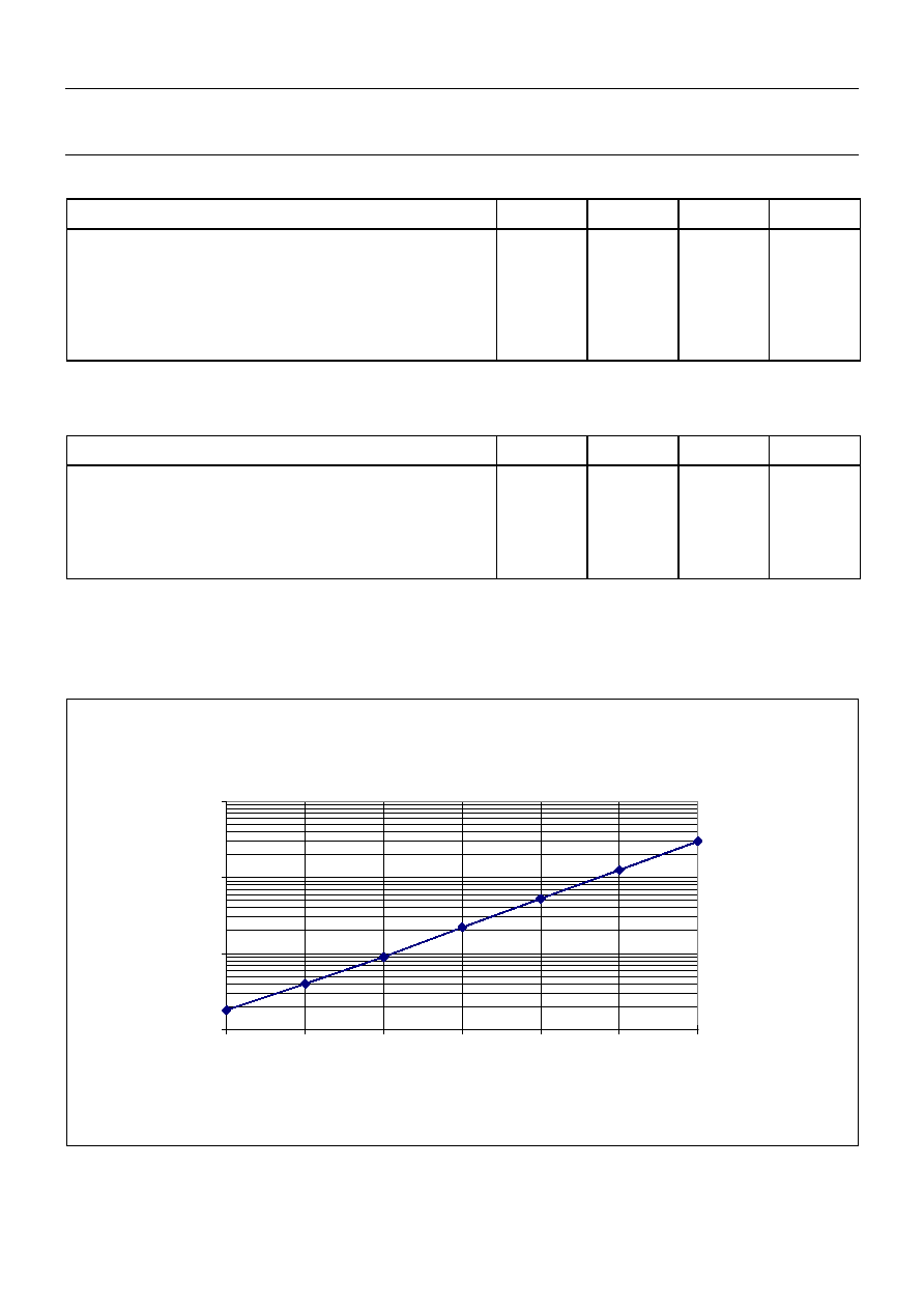
Figure 7 - Typical Linear dynamic range vs. horizontal read-out frequency and sensor temperature
LDR
Hor. Frequency (MHz)
Linear Dynamic Range
35ºC
45ºC
55ºC
0
2,000
4,000
6,000
8,000
10,000
12,000
14,000
16,000
18,000
20,000
0
5
10
15
20
25
30
35
40
LINEAR OPERATION
MIN.
TYPICAL
MAX.
UNIT
Linear dynamic range
1
Charge Transfer Efficiency
2
vertical
Charge Transfer Efficiency
2
horizontal
Image lag
Smear
3
Resolution (MTF) @ 42 lp/mm
Responsivity
Quantum efficiency @ 530 nm
White Shading
4
Random Non-Uniformity (RNU)
5
VNS required for good Vertical Anti-Blooming (VAB)
Power dissipation at 15 frames/s
4200:1
65
180
25
18
0.999995
0.999999
-39
250
30
0.3
24
410
0
0
2.5
5
28
%
dB
%
kel/lux·s
%
%
%
V
mW
1999 September
10
Philips Semiconductors
Product specification
Frame Transfer CCD Image Sensor
FTT1010-M
0
10
20
30
40
50
60
70
80
0
10
20
30
40
50
60
70
80
90
100
Figure 9 - Quantum efficiency versus wavelength
Figure 8 - Maximum number of images/second versus integration time
0
5
10
15
20
25
30
400
450
500
550
600
650
700
750
800
Images/sec.
Integration time (ms)
Maximum Read-out Speed
Quantum efficiency (%)
Wavelength (nm)
Quantum Efficiency
1 output
2 outputs
1999 September
11
Philips Semiconductors
Product specification
Frame Transfer CCD Image Sensor
FTT1010-M
1
Qmax is determined from the lowpass filtered image.
2
Qmax, shading is the maximum difference of the full-well charges of all pixels, relative to Qmax.
3
The linear full-well capacity Qlin is calculated from linearity test (see dynamic range). The evaluation test guarantees 97% linearity.
4
Charge handling capacity is the largest charge packet that can be transported through the register and read-out through the output buffer.
5
Overexposure over entire area while maintaining good Vertical Anti-Blooming (VAB). It is tested by measuring the dark line.
Figure 10 - Charge handling versus integration/transport voltage
Output Signal (k
el.)
Charge Handling vs. Integration/Transport Voltage
10V/14V
9V/13V
8V/12V
0
100
200
300
400
500
600
Exposure (arbitrary units)
1
2
3
4
5
6
LINEAR/SATURATION
MIN.
TYPICAL
MAX.
UNIT
Full-well capacity saturation level (Qmax)
1
Full-well capacity shading (Qmax, shading)
2
Full-well capacity linear operation (Qlin)
3
Charge handling capacity
4
Overexposure
5
handling
250
200
100
500
10
350
600
200
600
50
kel.
%
kel.
kel.
x Qmax level
1999 September
12
Philips Semiconductors
Product specification
Frame Transfer CCD Image Sensor
FTT1010-M
1
10
100
1000
0
10
20
30
40
50
60
1
FPN is the one-
value of the highpass image.
1
Matching of the four outputs is specified as
ACF with respect to reference measured at the operating point (Q
lin
/2).
Figure 11 - Dark current versus temperature
Dar
k Current (pA/cm
2
)
Dark Current
OUTPUT BUFFERS
MIN.
TYPICAL
MAX.
UNIT
Conversion factor
Mutual conversion factor matching (
ACF)
1
Supply current
Bandwidth
Output impedance buffer (R
load
= 3.3k
, C
load
= 2pF)
6
8
0
4
110
400
12
2
µV/el.
µV/el.
mA
MHz
DARK CONDITION
MIN.
TYPICAL
MAX.
UNIT
Dark current level @ 30
°
C
Dark current level @ 60
°
C
Fixed Pattern Noise
1
(FPN) @ 60
°
C
RMS readout noise @ 9MHz bandwidth after CDS
20
0.3
15
25
30
0.6
25
30
pA/cm
2
nA/cm
2
el.
el.
Temp. (
o
C)

1999 September
13
Philips Semiconductors
Product specification
Frame Transfer CCD Image Sensor
FTT1010-M
Application information
Current handling
One of the purposes of VPS is to drain the holes that are generated
during exposure of the sensor to light. Free electrons are either
transported to the VRD connection and, if excessive (from over-
exposure), free electrons are drained to VNS. No current should
flow into any VPS connection of the sensor. During high overexposure
a total current 10 to 15mA through all VPS connections together
may be expected. The PNP emitter follower in the circuit diagram
(figure 12) serves these current requirements.
VNS drains superfluous electrons as a result of overexposure. In
other words, it only sinks current. During high overexposure a total
current of 10 to 15mA through all VNS connections together may be
expected. The NPN emitter follower in the circuit diagram meets
these current requirements. The clamp circuit, consisting of the diode
and electrolytic capacitor, enables the addition of a Charge Reset
(CR) pulse on top of an otherwise stable VNS voltage. To protect the
CCD, the current resulting from this pulse should be limited. This
can be accomplished by designing a pulse generator with a rather
high output impedance.
Decoupling of DC voltages
All DC voltages (not VNS, which has additional CR pulses as
described above) should be decoupled with a 100nF decoupling
capacitor. This capacitor must be mounted as close as possible to
the sensor pin. Further noise reduction (by bandwidth limiting) is
achieved by the resistors in the connections between the sensor
and its voltage supplies. The electrons that build up the charge
packets that will reach the floating diffusions only add up to a small
current, which will flow through VRD. Therefore a large series resistor
in the VRD connection may be used.
Outputs
To limit the on-chip power dissipation, the output buffers are designed
with open source outputs. Outputs to be used should therefore be
loaded with a current source or more simply with a resistance to
GND. In order to prevent the output (which typically has an output
impedance of about 400
) from bandwidth limitation as a result of
capacitive loading, load the output with an emitter follower built from
a high-frequency transistor. Mount the base of this transistor as close
as possible to the sensor and keep the connection between the
emitter and the next stage short.
The CCD output buffer can easily be destroyed by ESD. By using
this emitter follower, this danger is suppressed; do NOT reintroduce
this danger by measuring directly on the output pin of the sensor
with an oscilloscope probe. Instead, measure on the output of the
emitter follower. Slew rate limitation is avoided by avoiding a too-
small quiescent current in the emitter follower; about 10mA should
do the job. The collector of the emitter follower should be decoupled
properly to suppress the Miller effect from the base-collector
capacitance.
A CCD output load resistor of 3.3k
typically results in a bandwidth
of 110MHz. The bandwidth can be enlarged to about 130MHz by
using a resistor of 2.2k
instead, which, however, also enlarges the
on-chip power dissipation.
Device protection
The output buffers of the FTT1010-M are likely to be damaged if
VPS rises above SFD or RD at any time. This danger is most realistic
during power-on or power-off of the camera. The RD voltage should
always be lower than the SFD voltage.
Never exceed the maximum output current. This may damage the
device permanently. The maximum output current should be limited
to 10mA. Be especially aware that the output buffers of these image
sensors are very sensitive to ESD damage.
Because of the fact that our CCDs are built on an n-type substrate,
we are dealing with some parasitic npn transistors. To avoid activation
of these transistors during switch-on and switch-off of the camera,
we recommend the application diagram of figure 12.
Unused sections
To reduce power consumption the following steps can be taken.
Connect unused output register pins (C1...C3, SG, OG) and unused
SFS pins to zero Volts.
More information
Detailed application information is provided in the application note
AN01 entitled `Camera Electronics for the mK x nK CCD Image
Sensor Family'.
1999 September
14
Philips Semiconductors
Product specification
Frame Transfer CCD Image Sensor
FTT1010-M
Figure 12 - Application diagram to protect the FTT1010-M
Device Handling
An image sensor is a MOS device which can be destroyed by electro-
static discharge (ESD). Therefore, the device should be handled
with care.
Always store the device with short-circuiting clamps or on conductive
foam. Always switch off all electric signals when inserting or removing
the sensor into or from a camera (the ESD protection in the CCD
image sensor process is less effective than the ESD protection of
standard CMOS circuits).
Being a high quality optical device, it is important that the cover
glass remain undamaged. When handling the sensor, use fingercots.
When cleaning the glass we recommend using ethanol (or possibly
water). Use of other liquids is strongly discouraged:
· if the cleaning liquid evaporates too quickly, rubbing is likely to
cause ESD damage.
· the cover glass and its coating can be damaged by other liquids.
Rub the window carefully and slowly.
Dry rubbing of the window may cause electro-static charges or
scratches which can destroy the device.
BAT74
Schottky!
VPS
SFD
VRD
BC
860C
BC
850C
VNS
+
-
1uF
100nF
100nF
100nF
100nF
2mA
BC
850C
0.5-1mA
27
15
10k
CR pulse
0
0.5-1mA
VCS
VOG
10k
10k
OUT
<7pF!
keep short
<10mm!
keep short!
output for
preprocessing
BFR
92A
1k
3.3k
10mA
100nF
100nF
100nF
BAT74
BAT74
0.5-1mA
BAT74
Schottky!
100
VSFD
1999 September
15
Philips Semiconductors
Product specification
Frame Transfer CCD Image Sensor
FTT1010-M
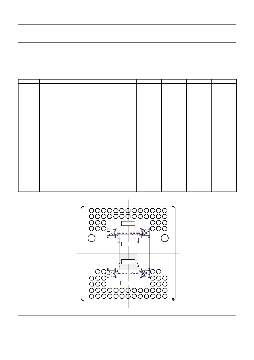
Pin configuration
The FTT1010-M is mounted in a Pin Grid Array (PGA) package with
76 pins in a 15x13 grid of 40.00 x 40.00 mm
2
. The position of pin A1
is marked with a gold dot on top of the package.
Figure 13 - FTT1010-M pin configuration (top view)
Symbol
Name
Pin # W
Pin # X
Pin # Y
Pin # Z
VNS
VNS
VNS
VNS
VNS
VPS
SFD
SFS
VCS
OG
RD
A1
A2
A3
A4
B1
B2
B3
B4
C1
C2
C3
SG
RG
OUT
NC
N substrate
N substrate
N substrate
N substrate
N substrate
P substrate
Source Follower Drain
Source Follower Source
Current Source
Output Gate
Reset Drain
Image Clock (Phase 1)
Image Clock (Phase 2)
Image Clock (Phase 3)
Image Clock (Phase 4)
Storage Clock (Phase 1)
Storage Clock (Phase 2)
Storage Clock (Phase 3)
Storage Clock (Phase 4)
Register Clock (Phase 1)
Register Clock (Phase 2)
Register Clock (Phase 3)
Summing Gate
Reset Gate
Output
Not connected
A12
D11
E11
E12
-
C11
A13
A10
A11
B13
B12
-
-
-
-
D13
C12
D12
C13
B9
B8
A8
B10
A9
B11
B7
A3
B2
D3
E2
E3
C3
A1
B5
A4
B1
B3
-
-
-
-
D1
C2
D2
C1
A6
A7
B6
A2
A5
B4
J2
F3
-
-
-
G3
J1
J4
J3
H1
H2
F1
G2
F2
G1
-
-
-
-
H5
H6
J6
H4
J5
H3
H7
F11
H12
J11
-
-
G11
J13
H9
J10
H13
H11
F13
G12
F12
G13
-
-
-
-
J8
J7
H8
J12
J9
H10
The clock phases of quadrant W are internally connected to X, and
the clock phases of Y are connected to Z.
J
H
G
F
E
D
C
B
A
J
H
G
F
E
D
C
B
A
SFD
VNS
VCS
SFS
RG
C2
C3
OG
RD
OUT
SG
C1
C2
NC
A4
A2
VPS
A1
A3
VNS
A4
A2
VPS
A1
A3
VNS
SFD
VNS
VCS
SFS
RG
C3
OG
RD
OUT
SG
C1
VNS
SFD
VNS
VCS
SFS
RG
C3
OG
RD
OUT
SG
C1
C2
VPS
VNS
B4
B2
VPS
B1
B3
VNS
SFD
NC
VCS
SFS
RG
C3
OG
RD
OUT
SG
C1
VNS
VNS
VNS
B4
B2
B1
B3
VNS
VNS
C2
VNS
1
2
3
4
5
6
7
8
9
10
11
12
13
1
2
3
4
5
6
7
8
9
10
11
12
13
B4
B1
B4
B1
IMAGE
TOP
Y
Z
X
W
FTT1010-M
STORAGE
1999 September
16
Philips Semiconductors
Product specification
Frame Transfer CCD Image Sensor
FTT1010-M
Package information
Figure 14 - Mechanical drawing of the PGA package of the FTT1010-M
A is the center of the image area.
Position of A:
26
± 0.15 to left edge of package
20 ± 0.10 to bottom of package
Angle of rotation: less than ± 1
0
Sensor flatness: < 7 µm (P-V)
Cover glass: Corning 7059
Thickness of cover glass: 1.00 ± 0.05
Refractive index: n
d
= 1.53
Single sided AR coating inside (430-660 nm)
All drawing units are in mm
Chip - bottom package 1.7 ± 0.15
1.4 / 100
COVER GLASS
SENSOR CRYSTAL
Chip - cover glass 1.3 ± 0.20
A ZONE
TOP VIEW
INDEX
MARK
PIN 1
40
±
0.40
26
±
0.15
1.27
±
0.15
8.9
0.46
±
0.05
(2.54)
STAND-OFF PIN
COVER GLASS
40
±
0.40
BOTTOM VIEW
Cover glass 1.0 ± 0.05
Image sensor chip
4.57
±
0.15
Top cover glass to top chip 2.4 ± 0.25
20
±
0.10
23
±
0.33
30.48
± 0.20
35.56 ± 0.20

Order codes
The sensors can be ordered using the following codes:
You can contact the Image Sensors division of Philips
Semiconductors at the following address:
Philips Semiconductors
Image Sensors
Internal Postbox WAG-05
Prof. Holstlaan 4
5656 AA Eindhoven
The Netherlands
phone
+31 - 40 - 27 44 400
fax
+31 - 40 - 27 44 090
www.semiconductors.philips.com/imagers/
Philips reser
v
es the r
ight to change an
y inf
o
r
mation contained herein without notice
.
All inf
o
r
mation fur
nished b
y
Philips is b
elie
v
ed to be accur
ate
.
© Philips Electronics N.V
.
1999
9922 157 35011
Philips
Semiconductors
FTT1010-M sensors
Description
Quality Grade
Order Code
FTT1010-M/TG
FTT1010-M/EG
FTT1010-M/IG
FTT1010-M/HG
Test grade
Economy grade
Industrial grade
High grade
9922 157 35031
9922 157 35051
9922 157 35021
9922 157 35011
TRAD
lmtb
Document Outline
- Description
- Device structure
- Architecture of the FTT1010-M
- Specifications
- Timing diagrams (for default operation)
- Performance
- Application information
- Device Handling
- Pin configuration
- Package information
- Order codes