GTL1655
16-bit LVTTL-to-GTL/GTL+ bus transceiver with live insertion

GTL1655
16-bit LVTTL-to-GTL/GTL+ bus transceiver with live insertion
Rev. 01 -- 11 May 2004
Product data
1.
Description
The GTL1655 is a 16-bit bus transceiver that incorporates HIGH-drive
LOW-output-impedance (100 mA/12
) with LVTTL-to-GTL/GTL+ and
GTL/GTL+-to-LVTTL logic level translation.
The device is configured as two 8-bit transceivers that share a common clock and a
master output enable pin, but also have individual latch timing and output enable
signals. D-type flip-flops and D-type latches enable three modes of data transfer;
Clocked, Latched, or Transparent. The GTL1655 provides the ideal interface between
cards operating at LVTTL levels and backplanes using GTL/GTL+ signal levels. The
combination of reduced output swing, reduced input threshold levels and configurable
edge control provides the higher speed operation of GTL/GTL+ backplanes.
The GTL1655 can be used at GTL (V
TT
= 1.2 V, V
REF
= 0.8 V) or GTL+ (V
TT
= 1.5 V,
V
REF
= 1.0 V) signalling levels. Port A and the control inputs are compliant with
LVTTL signal levels and are 5 V tolerant. Port B is designed to operate at GTL or
GTL+ signal levels, with V
REF
providing the reference voltage input.
The latch enable pins (nLEAB and nLEBA), the output enable pins (nOEAB, nOEBA)
and the clock pin (CP) are used to control the data flow through the two 8-bit
transceivers (n = 1 or 2). When nLEAB is set HIGH, the device will operate in the
transparent mode Port A to Port B. HIGH-to-LOW transitions of nLEAB will latch A
data independently of CP HIGH or LOW (latched mode). LOW-to-HIGH transitions of
CP will clock A data to the B port if nLEAB is LOW (clocked mode). Using the control
pins nLEBA, nOEBA and CP in the same way, data flow from Port B to Port A can be
controlled. The OE pin can be used to disable all of the I/O pins.
To optimize signal integrity, the GTL1655 features an adjustable edge rate control
(V
ERC
). By adjusting V
ERC
between GND and V
CC
, a designer can adjust the Port B
edge rate to suit an application's load conditions.
The GTL1655 permits true live insertion capability by incorporating:
�
BIAS V
CC
, to pre-charge outputs and avoid disturbing active data during card
insertion.
�
I
off
to disable current flow through powered-off I/Os.
�
Power-up 3-state, which ensures outputs are high-impedance during power-up,
thus preventing bus contention issues. Once V
CC
is above 1.5 V, the power-up
3-state circuit relinquishes control of the outputs to the OE pin. To ensure the
outputs remain 3-state, the OE pin should be tied to V
CC
via a pull-up resistor.

Philips Semiconductors
GTL1655
16-bit LVTTL-to-GTL/GTL+ bus transceiver with live insertion
Product data
Rev. 01 -- 11 May 2004
2 of 23
9397 750 12936
� Koninklijke Philips Electronics N.V. 2004. All rights reserved.
2.
Features
s
Combination of D-type latches and D-type flip-flops for transceiver operation in
clocked, latched or transparent mode
s
Logic level translation between LVTTL and GTL/GTL+ signals
s
HIGH-drive LOW-output-impedance (100 mA/12
) on Port B
s
Configurable rise and fall times on Port B
s
Supports live insertion (I
off
, Power-up 3-state, and BIAS V
CC
)
s
Bus Hold on Port A inputs
s
Over voltage tolerance on Port A
s
Minimized switching noise through use of distributed V
CC
and GND pins
s
Available in TSSOP64 package
s
Industrial temperature range (
-
40
�
C to +85
�
C)
s
ESD protection
x
HBM EIA/JESD22-A114-A exceeds 2000 V
x
CDM EIA/JESD22-C101 exceeds 1000 V
s
Latch-up EIA/JEDS78 exceeds 200 mA
3.
Quick reference data
Table 1:
Quick reference data
GND = 0 V; T
amb
= 25
�
C; t
r
= t
f
2.5 ns
Symbol
Parameter
Conditions
Min
Typ
Max
Unit
t
PLH
propagation delay, nAn to nBn
V
CC
= 3.3 V; V
ERC
= GND;
V
TT
= 1.5 V; V
REF
= 1 V
-
3.9
-
ns
V
CC
= 3.3 V; V
ERC
= GND;
V
TT
= 1.5 V; V
REF
= 1 V
-
4.4
-
ns
propagation delay, nBn to nAn
V
CC
= 3.3 V
-
2.6
-
ns
t
PHL
propagation delay, nAn to nBn
V
CC
= 3.3 V; V
ERC
= GND;
V
TT
= 1.5 V; V
REF
= 1 V
-
3.1
-
ns
V
CC
= 3.3 V; V
ERC
= GND;
V
TT
= 1.5 V; V
REF
= 1 V
-
2.7
-
ns
propagation delay, nBn to nAn
V
CC
= 3.3 V
-
4.2
-
ns
C
i
input capacitance (control pins)
V
i
= V
CC
or GND
-
3
-
pF
C
I/O
I/O capacitance, Port A
V
i
= V
CC
or GND
-
7
-
pF
I/O capacitance, Port B
V
i
= V
CC
or GND
-
8
-
pF

Philips Semiconductors
GTL1655
16-bit LVTTL-to-GTL/GTL+ bus transceiver with live insertion
Product data
Rev. 01 -- 11 May 2004
3 of 23
9397 750 12936
� Koninklijke Philips Electronics N.V. 2004. All rights reserved.
4.
Ordering information
Standard packing quantities and other packaging data are available at
www.philipslogic.com/packaging.
4.1 Ordering options
Table 2:
Ordering information
Type number
Package
Name
Description
Version
GTL1655DGG
TSSOP64
plastic thin shrink small outline package; 64 leads;
body width 6.1 mm
SOT646-1
Table 3:
Part marking
Type number
Topside mark
Temperature range
GTL1655DGG
GTL1655DGG
T
amb
=
-
40
�
C to +85
�
C
Philips Semiconductors
GTL1655
16-bit LVTTL-to-GTL/GTL+ bus transceiver with live insertion
Product data
Rev. 01 -- 11 May 2004
4 of 23
9397 750 12936
� Koninklijke Philips Electronics N.V. 2004. All rights reserved.
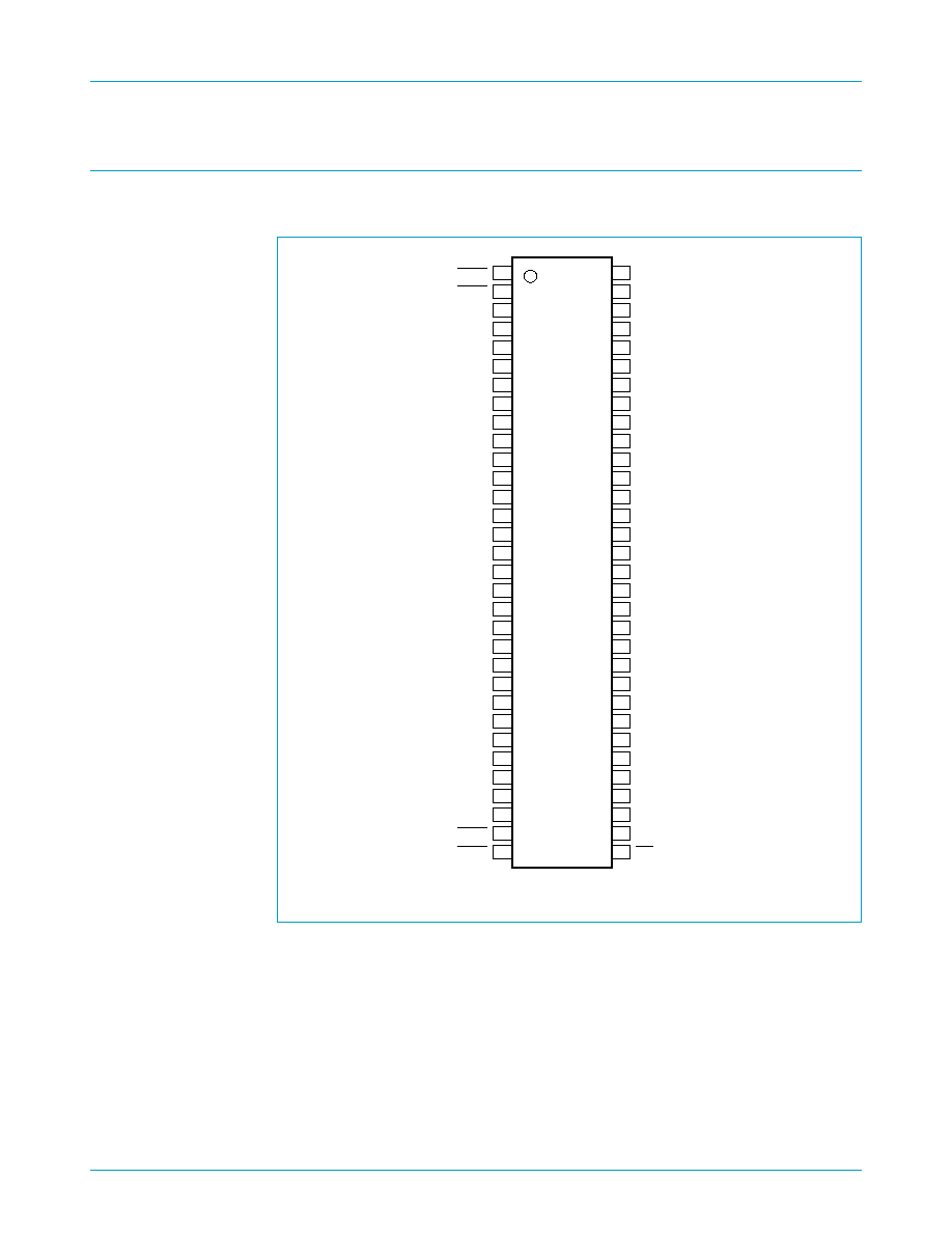
5.
Pinning information
5.1 Pinning
Fig 1.
TSSOP64 pin configuration.
GTL1655DGG
1OEAB
CP
1OEBA
1LEAB
V
CC
1LEBA
1A1
V
ERC
GND
GND
1A2
1B1
1A3
1B2
GND
GND
1A4
1B3
GND
1B4
1A5
1B5
GND
GND
1A6
1B6
1A7
1B7
V
CC
V
CC
1A8
1B8
2A1
2B1
GND
GND
2A2
2B2
2A3
2B3
GND
GND
2A4
2B4
2A5
2B5
GND
V
REF
2A6
2B6
GND
GND
2A7
2B7
V
CC
2B8
2A8
BIAS_V
CC
GND
2LEAB
2OEAB
2LEBA
2OEBA
002aaa763
OE
1
2
3
4
5
6
7
8
9
10
11
12
13
14
15
16
17
18
19
20
21
22
23
24
25
26
27
28
29
30
31
32
64
63
62
61
60
59
58
57
56
55
54
53
52
51
50
49
48
47
46
45
44
43
42
41
40
39
38
37
36
35
34
33

Philips Semiconductors
GTL1655
16-bit LVTTL-to-GTL/GTL+ bus transceiver with live insertion
Product data
Rev. 01 -- 11 May 2004
5 of 23
9397 750 12936
� Koninklijke Philips Electronics N.V. 2004. All rights reserved.
5.2 Pin description
Table 4:
Pin description
Symbol
Pin
Description
1OEAB
1
output enable 1A-to-1B (active-LOW)
1OEBA
2
output enable 1B-to-1A (active-LOW)
V
CC
3, 15, 28, 50
DC supply voltage
1A1 to 1A8
4, 6, 7, 9, 11, 13,
14, 16
data inputs/outputs port 1A
GND
5, 8, 10, 12, 18,
21, 24, 26, 30,
39, 44, 47, 53,
57, 60
ground (0 V)
2A1 to 2A8
17, 19, 20, 22,
23, 25, 27, 29
data inputs/outputs port 2A
2OEAB
31
output enable 2A-to-2B (active-LOW)
2OEBA
32
output enable 2B-to-2A (active-LOW)
OE
33
output enable, all I/O pins (active-LOW)
2LEBA
34
latch enable 2B-to-2A
2LEAB
35
latch enable 2A-to-2B
BIAS_V
CC
36
bias supply voltage
2B8 to 2B1
37, 38, 40, 42,
43, 45, 46, 48
data inputs/outputs port 2B
V
REF
41
reference voltage
1B8 to 1B1
49, 51, 52, 54,
55, 56, 58, 59
data inputs/outputs port 1B
V
ERC
61
edge-rate control voltage Port B
1LEBA
62
latch enable 2B-to-2A
1LEAB
63
latch enable 1A-to-1B
CP
64
clock input
Philips Semiconductors
GTL1655
16-bit LVTTL-to-GTL/GTL+ bus transceiver with live insertion
Product data
Rev. 01 -- 11 May 2004
6 of 23
9397 750 12936
� Koninklijke Philips Electronics N.V. 2004. All rights reserved.
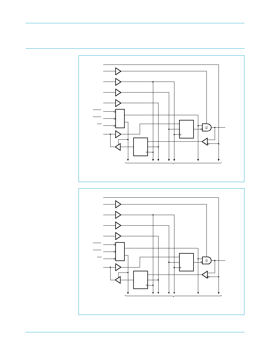
6.
Functional description
Fig 2.
Logic diagram.
Fig 3.
Logic diagram.
1D
C1
CP
41
61
64
63
62
V
REF
V
ERC
CP
1LEAB
1LEBA
2
1OEBA
1
1OEAB
33
OE
4
1A1
1D
C1
CP
TO 7 OTHER CHANNELS
59
1B1
002aaa764
1D
C1
CP
41
61
64
35
34
V
REF
V
ERC
CP
2LEAB
2LEBA
32
2OEBA
31
2OEAB
33
OE
17
2A1
1D
C1
CP
TO 7 OTHER CHANNELS
48
2B1
002aaa765
Philips Semiconductors
GTL1655
16-bit LVTTL-to-GTL/GTL+ bus transceiver with live insertion
Product data
Rev. 01 -- 11 May 2004
7 of 23
9397 750 12936
� Koninklijke Philips Electronics N.V. 2004. All rights reserved.
6.1 Function table
[1]
A-to-B data flow is shown. B-to-A is similar, but uses OEBA, LEBA, and CP. It is not recommended to
set OEAB and OEBA LOW at the same time.
X -- don't care
H -- HIGH voltage level
L -- LOW voltage level
Z -- high-impedance OFF-state
-- LOW-to-HIGH transition
[2]
Output level before the indicated steady-state input conditions were established, provided that CP
was HIGH before LEAB went LOW.
[3]
Output level before the indicated steady-state input conditions were established.
Table 5:
Function table
See
Table note [1]
.
Inputs
Output
Mode
OEAB
LEAB
CP
Port A
Port B
H
X
X
X
Z
isolation
L
H
X
L
L
transparent
L
H
X
H
H
transparent
L
L
L
L
registered
L
L
H
H
registered
L
L
H
X
B0
[2]
previous state
L
L
L
X
B0
[3]
previous state
Table 6:
Output Enable function table
See
Table note [1]
.
Inputs
Outputs
OE
OEAB
OEBA
Port A
Port B
L
L
L
active
active
L
L
H
Z
active
L
H
L
active
Z
L
H
H
Z
Z
H
X
X
Z
Z
Table 7:
Port B edge-rate control (V
ERC
) function table
See
Table note [1]
.
Input V
ERC
Output port B edge-rate
Logic level
Nominal voltage
H
V
CC
slow
L
GND
fast

Philips Semiconductors
GTL1655
16-bit LVTTL-to-GTL/GTL+ bus transceiver with live insertion
Product data
Rev. 01 -- 11 May 2004
8 of 23
9397 750 12936
� Koninklijke Philips Electronics N.V. 2004. All rights reserved.
7.
Limiting values
[1]
Stresses beyond those listed may cause permanent damage to the device. These are stress ratings only and functional operation of the
device at these or any conditions beyond those indicated under
Section 8 "Recommended operating conditions"
is not implied.
Exposure to absolute-maximum-rated conditions for extended periods may affect device reliability.
[2]
The performance capability of a high-performance integrated circuit in conjunction with its thermal environment can create junction
temperatures which are detrimental to reliability. The maximum junction temperature of this integrated circuit should not exceed 150
�
C.
[3]
The input and output negative voltage ratings may be exceeded if the input and output clamp current ratings are observed.
Table 8:
Limiting values
In accordance with the Absolute Maximum Rating System (IEC 60134). See
Table note [1]
and
Table note [2]
Symbol
Parameter
Conditions
Min
Max
Unit
V
CC
DC supply voltage
-
0.5
+4.6
V
BIAS V
CC
BIAS supply voltage
-
0.5
+4.6
V
I
IK
input clamping diode current
V
i
< 0 V
-
-
50
mA
V
i
DC input voltage
port A
[3]
-
0.5
+7.0
V
port B; V
ERC
, V
REF
[3]
-
0.5
+4.6
V
V
o
DC output voltage
output in HIGH or power-OFF state;
port A
-
0.5
+7.0
V
output in HIGH or power-OFF state;
port B
-
0.5
+4.6
V
I
OL(d)
DC LOW-level diode output current
port A
-
48
mA
port B
-
200
mA
I
OH(d)
DC HIGH-level diode output current
port A
-
48
mA
T
stg
storage temperature
-
65
+150
�
C

Philips Semiconductors
GTL1655
16-bit LVTTL-to-GTL/GTL+ bus transceiver with live insertion
Product data
Rev. 01 -- 11 May 2004
9 of 23
9397 750 12936
� Koninklijke Philips Electronics N.V. 2004. All rights reserved.
8.
Recommended operating conditions
Table 9:
Recommended operating conditions
Symbol
Parameter
Conditions
Min
Max
Unit
BIAS V
CC
DC supply voltage
3.0
3.6
V
V
TT
termination voltage
GTL
1.14
1.26
V
GTL+
1.35
1.65
V
V
REF
GTL reference voltage
GTL
0.74
0.87
V
GTL+
0.87
1.10
V
V
i
input voltage
port B
0
V
TT
V
except port B
0
5.5
V
V
IH
HIGH-level input voltage
port B
V
REF
+ 50 mV
-
V
except port B
2.0
-
V
V
ERC
V
CC
-
0.6
-
V
V
IL
LOW-level input voltage
port B
-
V
REF
-
50 mV
V
except port B
-
0.8
V
V
ERC
-
0.6
V
|
I
IK
|
input clamp current
-
18
mA
I
OH
HIGH-level output current
port A
-
-
24
mA
I
OL
LOW-level output current
port A
-
24
mA
port B
-
100
mA
t/
V
CC
power-up ramp rate
200
-
�
s/V
T
amb
operating ambient temperature
-
40
85
�
C

Philips Semiconductors
GTL1655
16-bit LVTTL-to-GTL/GTL+ bus transceiver with live insertion
Product data
Rev. 01 -- 11 May 2004
10 of 23
9397 750 12936
� Koninklijke Philips Electronics N.V. 2004. All rights reserved.
9.
Static characteristics
Table 10:
DC characteristics
T
amb
=
-
40
�
C to +85
�
C; values otherwise stated V
REF
= 1 V; V
TT
= 1.5 V.
Symbol
Parameter
Conditions
Min
Typ
[1]
Max
Unit
V
IK
input clamp voltage
V
CC
= 3.0 V; I
IK
= 19 mA
-
-
-
1.2
V
V
OH
HIGH-level output
voltage
port A
V
CC
= 3.0 V to 3.6 V;
I
OH
=
-
100
�
A
V
CC
-
0.2 -
-
V
V
CC
= 3.0 V;
I
OH
=
-
12 mA
2.4
-
-
V
V
CC
= 3.0 V;
I
OH
=
-
24 mA
2.2
-
-
V
V
OL
LOW-level output
voltage
port A
V
CC
= 3.0 to 3.6 V;
I
OL
= 100
�
A
-
-
0.2
V
V
CC
= 3.0 V;
I
OL
= 12 mA
-
-
0.4
V
V
CC
= 3.0 V;
I
OL
= 24 mA
-
-
0.55
V
port B
V
CC
= 3.0 V;
I
OL
= 40 mA
-
-
0.2
V
V
CC
= 3.0 V;
I
OL
= 80 mA
-
-
0.4
V
V
CC
= 3.0 V;
I
OL
= 100 mA
-
-
0.5
V
I
i
input leakage current
control pins
V
CC
= 3.6 V;
V
i
= V
CC
or GND
-
-
�
10
�
A
port B
V
CC
= 3.6 V;
V
i
= V
TT
or GND
-
-
�
10
�
A
I
off
output OFF current
port A +
control pin
V
CC
= 0 V;
V
o
= 0 V to 3.6 V
-
-
�
100
�
A
port B
V
CC
= 0 V;
V
o
= 0 V to 1.5 V
-
-
�
300
�
A
I
HOLD
bus hold current,
A outputs
port A
V
CC
= 3.0 V;
V
i
= 0.8 V
75
-
-
�
A
V
CC
= 3.0 V;
V
i
= 2.0 V
-
75
-
-
�
A
overdrive current
port A
V
CC
= 3.6 V;
V
i
= 0 V to V
CC
[2]
-
-
�
500
�
A
I
OZH
HIGH OFF-state output
current
port B
V
CC
= 3.6 V;
V
o
= 1.5 V
-
-
10
�
A
I
OZL
LOW OFF-state
output current
port B
V
CC
= 3.6 V;
V
o
= 0.4 V
-
-
-
10
�
A
I
OZ
OFF-state output
current
port A
V
CC
= 3.6 V;
V
o
= V
CC
or GND
[3]
-
-
10
�
A
I
OZPU
power-up 3-state output
current
V
CC
= 0 to 3.6 V; V
o
= 0.5 V to 3 V;
OE = LOW
-
-
�
50
�
A
I
OZPD
power-down 3-state
output current
V
CC
= 3.6 to 0 V; V
o
= 0.5 V to 3 V;
OE = LOW
-
-
�
50
�
A

Philips Semiconductors
GTL1655
16-bit LVTTL-to-GTL/GTL+ bus transceiver with live insertion
Product data
Rev. 01 -- 11 May 2004
11 of 23
9397 750 12936
� Koninklijke Philips Electronics N.V. 2004. All rights reserved.
[1]
All typical values are measured at V
CC
= 3.3 V and T
amb
= 25
�
C.
[2]
This is the bus-hold maximum dynamic current. It is the minimum overdrive current required to switch the input from one state to
another.
[3]
For I/O ports, this parameter I
OZ
includes the input leakage current.
[4]
This is the increase in supply current for each input that is at the specified TTL voltage level rather than V
CC
or GND.
I
CC
quiescent supply
current
outputs
HIGH
V
CC
= 3.6 V;
V
i
= V
CC
or GND;
I
o
= 0 mA
-
-
45
mA
outputs
LOW
V
CC
= 3.6 V;
V
i
= V
CC
or GND;
I
o
= 0 mA
-
-
45
mA
disabled
V
CC
= 3.6 V;
V
i
= V
CC
or GND;
I
o
= 0 mA
-
-
45
mA
I
CC
additional quiescent
supply current per input
pin; except port B
V
CC
= 3.6 V; one input at
V
CC
-
0.6 V; port A or control inputs
at V
CC
or GN D
[4]
-
0.1
-
mA
C
i
input capacitance
control pins
V
CC
= 3.6 V;
V
i
= V
CC
or 0
-
3
5
pF
C
IO
I/O capacitance
port A
V
CC
= 3.6 V;
V
i
= V
CC
or 0
-
7
8
pF
port B
V
CC
= 3.6 V;
V
i
= V
CC
or 0
-
8
10
pF
Table 10:
DC characteristics
...continued
T
amb
=
-
40
�
C to +85
�
C; values otherwise stated V
REF
= 1 V; V
TT
= 1.5 V.
Symbol
Parameter
Conditions
Min
Typ
[1]
Max
Unit
Table 11:
Live insertion characteristics
T
amb
=
-
40
�
C to +85
�
C
Symbol
Parameter
Conditions
Min
Typ
Max
Unit
I
CC
(BIAS V
CC
)
supply current
V
CC
= 0 V to 3.0 V; V (port B) = 0 to 1.2 V;
V
i
(BIAS V
CC
) = 3.0 V to 3.6 V
-
-
5
mA
V
CC
= 3.0 V to 3.6 V;
V (port B) = 0 to 1.2 V;
V
i
(BIAS V
CC
) = 3.0 V to 3.6 V
-
-
10
�
A
V
o
output voltage
port B
V
CC
= 0 V;
V
i
(BIAS V
CC
) = 3.3 V
1
-
1.2
V
I
o
output current
port B
V
CC
= 0 V; V (port B) = 0.4 V;
V
i
(BIAS V
CC
) = 3 V to 3.6 V
-
1
-
-
�
A
V
CC
= 0 V to 3.6 V; OE = 3.3 V;
V (port B) = 0 V to 1.5 V
-
-
300
�
A
V
CC
= 0 V to 1.5 V;
OE = 0 V to 3.3 V;
V (port B) = 0 V to 1.5 V
-
-
300
�
A
Philips Semiconductors
GTL1655
16-bit LVTTL-to-GTL/GTL+ bus transceiver with live insertion
Product data
Rev. 01 -- 11 May 2004
12 of 23
9397 750 12936
� Koninklijke Philips Electronics N.V. 2004. All rights reserved.
10. Dynamic characteristics
Table 12:
Timing requirements over recommended supply voltage
V
TT
= 1.2 V; V
REF
= 0.8 V and V
ERC
= V
CC
or GND for GTL (unless otherwise noted; see Figures
15
and
16
).
T
amb
=
-
40
�
C to +85
�
C.
Symbol
Parameter
Conditions
Min
Typ
Max
Unit
t
W
pulse duration
CP HIGH or LOW; see Figures
4
and
5
3.0
-
-
ns
LE HIGH; see Figures
6
and
7
3.0
-
-
ns
t
su
set-up time
data before CP
; see Figures
4
and
5
2.7
-
-
ns
data before LE
;
see Figures
6
and
7
2.8
-
-
ns
t
h
hold time
data after CP
; see Figures
4
and
5
0.4
-
-
ns
data after LE
;
see Figures
6
and
7
1.2
-
-
ns
Table 13:
Port A to Port B switching
V
TT
= 1.2 V; V
REF
= 0.8 V and V
ERC
= V
CC
or GND for GTL (see
Figure 16
).
T
amb
=
-
40
�
C to +85
�
C.
Symbol
Parameter
Conditions
Min
Typ
Max
Unit
t
PLH
A to B
OEAB = OE = 0 V;
LEAB = 3 V
V
ERC
= V
CC
;
see
Figure 10
3.1
5.3
6.2
ns
t
PHL
2.2
3.8
6.2
ns
t
PLH
CP to B
OEAB = OE = 0 V;
LEAB = 0 V
V
ERC
= V
CC
;
see
Figure 4
3.4
5.9
7.2
ns
t
PHL
2.4
4.1
6.0
ns
t
PLH
LEAB to B
OEAB = OE = 0 V;
CP = 0 or 3 V
V
ERC
= V
CC
;
see
Figure 8
3.3
5.7
7.0
ns
t
PHL
2.6
4.6
6.8
ns
t
PLH
OEAB or OE to B
LEAB = 3.0 V;
Port A = 0 V
V
ERC
= V
CC
;
see
Figure 12
2.7
5.3
6.5
ns
t
PHL
2.5
3.9
6.4
ns
t
PLH
A to B
OEAB = OE = 0 V;
LEAB = 3 V
V
ERC
= GND;
see
Figure 10
2.3
4.4
5.3
ns
t
PHL
1.7
2.7
4.4
ns
t
PLH
CP to B
OEAB = OE = 0 V;
LEAB = 0 V
V
ERC
= GND;
see
Figure 4
2.7
5.2
6.1
ns
t
PHL
1.8
3.7
5.3
ns
t
PLH
LEAB to B
OEAB = OE = 0 V;
CP = 0 or 3 V
V
ERC
= GND;
see
Figure 8
2.5
4.8
6.5
ns
t
PHL
2.0
3.6
5.3
ns
t
PLH
OEAB or OE to B
LEAB = 3.0 V;
Port A = 0 V
V
ERC
= GND;
see
Figure 12
2.0
4.8
6.2
ns
t
PHL
2.0
3.1
4.9
ns
V/
t
output slew rate
0.6 V to 1.0 V
V
ERC
= V
CC
-
-
1
V/ns
V
ERC
= GND
-
-
1
V/ns
t
sk(o)
output edge skew
measured at V
REF
-
-
1
ns

Philips Semiconductors
GTL1655
16-bit LVTTL-to-GTL/GTL+ bus transceiver with live insertion
Product data
Rev. 01 -- 11 May 2004
13 of 23
9397 750 12936
� Koninklijke Philips Electronics N.V. 2004. All rights reserved.
Table 14:
Port B to Port A switching
V
TT
= 1.2 V; V
REF
= 0.8 V for GTL (see
Figure 15
).
T
amb
=
-
40
�
C to +85
�
C.
Symbol
Parameter
Conditions
Min
Typ
Max
Unit
f
max
maximum
frequency
160
-
-
MHz
t
PLH
B to A
OEBA = OE = 0 V;
LEBA = 3 V
see
Figure 11
1.8
2.6
4.9
ns
t
PHL
2.3
4.2
5.3
ns
t
PLH
CP to A
OEBA = OE = 0 V;
LEBA = 0 V
see
Figure 5
1.5
3.1
4.4
ns
t
PHL
1.5
3.7
4.6
ns
t
PLH
LEBA to A
OEBA = OE = 0 V
see
Figure 9
1.3
2.7
4.0
ns
t
PHL
1.4
3.1
3.9
ns
t
PZL
OEBA or OE to A
LEBA = 3.0 V;
Port B = 0 V
see
Figure 13
1.3
3.1
5.1
ns
t
PLZ
1.7
2.8
6.1
ns
t
PZH
LEBA = 3 V;
Port B = V
TT
see
Figure 14
1.3
3.3
5.1
ns
t
PHZ
1.7
3.3
6.1
ns
t
sk(o)
output edge skew
measured at 1.5 V
-
-
1
ns

Philips Semiconductors
GTL1655
16-bit LVTTL-to-GTL/GTL+ bus transceiver with live insertion
Product data
Rev. 01 -- 11 May 2004
14 of 23
9397 750 12936
� Koninklijke Philips Electronics N.V. 2004. All rights reserved.
Table 15:
Timing requirements over recommended supply voltage
V
TT
= 1.5 V; V
REF
= 1 V and V
ERC
= V
CC
or GND for GTL+ (unless otherwise noted).
T
amb
=
-
40
�
C to +85
�
C.
Symbol
Parameter
Conditions
Min
Typ
Max
Unit
t
W
pulse duration
CP HIGH or LOW; see Figures
4
and
5
3.0
-
-
ns
LE HIGH; see Figures
6
and
7
3.0
-
-
ns
t
su
set-up time
data before CP
; see Figures
4
and
5
2.7
-
-
ns
data before LE
;
see Figures
6
and
7
2.8
-
-
ns
t
h
hold time
data after CP
; see Figures
4
and
5
0.4
-
-
ns
data after LE
;
see Figures
6
and
7
1.2
-
-
ns
Table 16:
Port A to Port B switching
V
TT
= 1.5 V; V
REF
= 1 V and V
ERC
= V
CC
or GND for GTL+ (see Figures
15
and
16
).
T
amb
=
-
40
�
C to +85
�
C.
Symbol
Parameter
Conditions
Min
Typ
Max
Unit
t
PLH
A to B
OEAB = OE = 0 V;
LEAB = 3 V
V
ERC
= V
CC
;
see
Figure 10
3.0
4.7
6.1
ns
t
PHL
2.3
4.4
6.5
ns
t
PLH
CP to B
OEAB = OE = 0 V;
LEAB = 0 V
V
ERC
= V
CC
;
see
Figure 4
3.3
5.3
7.0
ns
t
PHL
2.7
4.7
6.2
ns
t
PLH
LEAB to B
OEAB = OE = 0 V;
CP = 0 or 3 V
V
ERC
= V
CC
;
see
Figure 8
3.2
5.2
6.8
ns
t
PHL
2.8
5.2
7.1
ns
t
PLH
OEAB or OE to B
LEAB = 3.0 V;
Port A = 0 V
V
ERC
= V
CC
;
see
Figure 12
3.2
4.8
6.5
ns
t
PHL
2.6
4.6
6.6
ns
t
PLH
A to B
OEAB = OE = 0 V;
LEAB = 3 V
V
ERC
= GND;
see
Figure 10
2.3
3.9
5.2
ns
t
PHL
1.7
3.1
4.5
ns
t
PLH
CP to B
OEAB = OE = 0 V;
LEAB = 0 V
V
ERC
= GND;
see
Figure 4
2.5
4.8
6.0
ns
t
PHL
1.9
4.1
5.4
ns
t
PLH
LEAB to B
OEAB = OE = 0 V;
CP = 0 or 3 V
V
ERC
= GND;
see
Figure 8
2.5
4.3
6.5
ns
t
PHL
2.1
4.0
5.4
ns
t
PLH
OEAB or OE to B
LEAB = 3.0 V;
Port A = 0 V
V
ERC
= GND;
see
Figure 12
2.1
4.4
6.1
ns
t
PHL
2.0
3.4
5.0
ns
V/
t
output slew rate
0.6 V to 1.3 V
V
ERC
= V
CC
-
-
1
V/ns
V
ERC
= GND
-
-
1
V/ns
t
sk(o)
output edge skew
measured at V
REF
-
-
1
ns
Philips Semiconductors
GTL1655
16-bit LVTTL-to-GTL/GTL+ bus transceiver with live insertion
Product data
Rev. 01 -- 11 May 2004
15 of 23
9397 750 12936
� Koninklijke Philips Electronics N.V. 2004. All rights reserved.
10.1 AC waveforms
Table 17:
Port B to Port A switching
V
TT
= 1.5 V; V
REF
= 1 V for GTL+ (see Figures
15
and
16
).
T
amb
=
-
40
�
C to +85
�
C.
Symbol
Parameter
Conditions
Min
Typ
Max
Unit
f
max
maximum
frequency
160
-
-
MHz
t
PLH
B to A
OEBA = OE = 0 V;
LEBA = 3 V
see
Figure 11
1.8
2.6
4.9
ns
t
PHL
2.3
4.2
5.3
ns
t
PLH
CP to A
OEBA = OE = 0 V;
LEBA = 0 V
see
Figure 5
1.5
3.1
4.4
ns
t
PHL
1.5
3.7
4.6
ns
t
PLH
LEBA to A
OEBA = OE = 0 V
see
Figure 9
1.3
2.7
4.0
ns
t
PHL
1.4
3.1
3.9
ns
t
PZL
OEBA or OE to A
LEBA = 3.0 V;
Port B = 0 V
see
Figure 13
1.3
3.1
5.1
ns
t
PLZ
1.7
2.8
6.1
ns
t
PZH
LEBA = 3 V;
Port B = V
TT
see
Figure 14
1.3
3.3
5.1
ns
t
PHZ
1.7
3.3
6.1
ns
t
sk(o)
output edge skew
measured at 1.5 V
-
-
1
ns
Test condition: OEAB = OE = 0 V
Test condition: OEAB = OE = 0 V; LEBA = 0 V
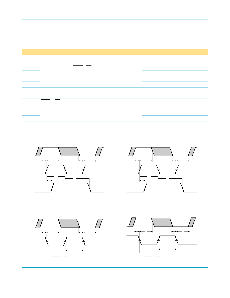
Fig 4.
CP to B timing.
Fig 5.
CP to A timing.
Test condition: OEAB = OE = 0 V
Test condition: OEAB = OE = 0 V
Fig 6.
LEAB set-up and hold times.
Fig 7.
LEBA set-up and hold times.
002aaa766
3.0 V
0 V
V
TT
V
OL
t
PLH
t
PHL
V
REF
V
REF
1.5 V
1.5 V
1.5 V
t
W
CP
input
Port B
output
t
W
1.5 V
1.5 V
1.5 V
t
su
t
h
t
su
Port A
input
t
h
1.5 V
0 V
3.0 V
002aaa767
3.0 V
0 V
V
OH
V
OL
t
PLH
t
PHL
1.5 V
1.5 V
1.5 V
1.5 V
1.5 V
t
W
CP
input
Port A
output
t
W
V
REF
t
su
t
h
t
su
Port B
input
t
h
V
REF
0 V
V
TT
V
REF
V
REF
002aaa768
3.0 V
0 V
1.5 V
1.5 V
1.5 V
t
W
LEAB
input
1.5 V
1.5 V
1.5 V
t
su
t
h
t
su
Port A
input
t
h
1.5 V
0 V
3.0 V
002aaa769
3.0 V
0 V
1.5 V
1.5 V
1.5 V
t
W
LEBA
input
V
REF
t
su
t
h
t
su
Port B
input
t
h
V
REF
0 V
V
TT
V
REF
V
REF
Philips Semiconductors
GTL1655
16-bit LVTTL-to-GTL/GTL+ bus transceiver with live insertion
Product data
Rev. 01 -- 11 May 2004
16 of 23
9397 750 12936
� Koninklijke Philips Electronics N.V. 2004. All rights reserved.
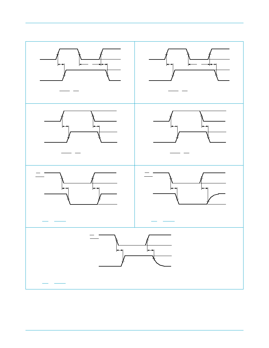
Test condition: OEAB = OE = 0 V; CP = 0 V or 3 V
Test condition: OEAB = OE = 0 V; CP = 0 V or 3 V
Fig 8.
LEAB to B propagation delay.
Fig 9.
LEBA to A propagation delay.
Test conditions: OEAB = OE = 0 V; LEAB = 3 V
Test conditions: OEBA = OE = 0 V; LEBA = 3 V
Fig 10. A to B propagation delay.
Fig 11. B to A propagation delay.
Test conditions: LEAB = 3 V; Port A = 0 V
Test conditions: LEBA = 3 V; Port B = 0 V
Fig 12. OE or OEAB to B propagation delay.
Fig 13. OE or OEBA to A propagation delay.
Test conditions: LEBA = 3 V; Port B = V
TT
Fig 14. OE or OEBA to A propagation delay.
002aaa770
3.0 V
0 V
V
TT
V
OL
t
PLH
t
PHL
V
REF
V
REF
1.5 V
1.5 V
1.5 V
t
W
LEAB
input
Port B
output
002aaa771
3.0 V
0 V
V
OH
V
OL
t
PLH
t
PHL
1.5 V
1.5 V
1.5 V
1.5 V
1.5 V
t
W
LEBA
input
Port A
output
002aaa772
3.0 V
0 V
V
TT
V
OL
t
PLH
t
PHL
V
REF
V
REF
1.5 V
1.5 V
Port A
input
Port B
input
002aaa773
V
TT
0 V
V
OH
V
OL
t
PLH
t
PHL
1.5 V
1.5 V
V
REF
V
REF
Port B
input
Port A
input
002aaa774
3.0 V
0 V
V
TT
V
OL
t
PHL
t
PLH
V
REF
V
REF
1.5 V
1.5 V
OE or
OEAB
input
Port B
output
002aaa775
3.0 V
0 V
3.0 V
V
OL
t
PZL
t
PLZ
V
OL
+ 0.3 V
1.5 V
1.5 V
1.5 V
OE or
OEBA
input
Port A
output
002aaa776
3.0 V
0 V
V
OH
0 V
t
PZH
t
PHZ
V
OH
-
0.3 V
1.5 V
1.5 V
1.5 V
OE or
OEBA
input
Port A
output
Philips Semiconductors
GTL1655
16-bit LVTTL-to-GTL/GTL+ bus transceiver with live insertion
Product data
Rev. 01 -- 11 May 2004
17 of 23
9397 750 12936
� Koninklijke Philips Electronics N.V. 2004. All rights reserved.
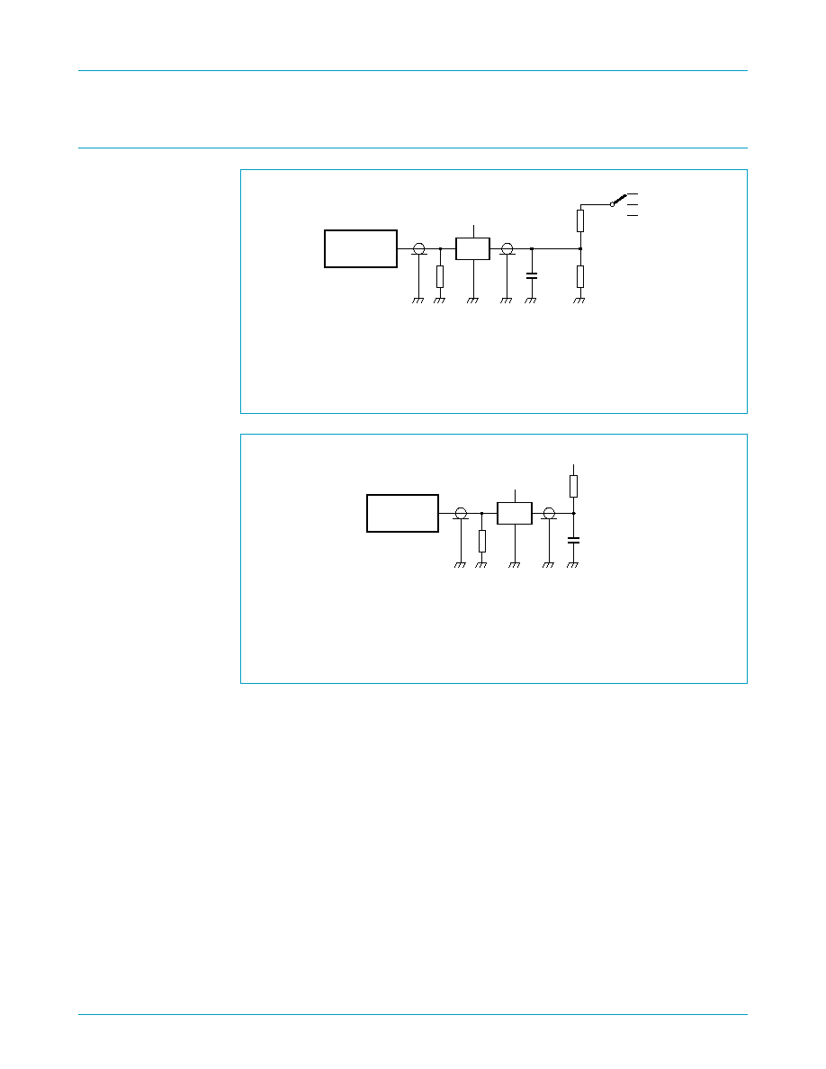
11. Test information
R
L
= Load resistor.
C
L
= Load capacitance including jig and probe capacitance.
R
T
= Termination resistance should be equal to the output impedance Z
O
of the pulse
generator.
Fig 15. Load circuitry for Port A output switching times.
R
L
= Load resistor.
C
L
= Load capacitance including jig and probe capacitance.
R
T
= Termination resistance should be equal to the output impedance Z
O
of the pulse
generator.
Fig 16. Load circuitry for Port B output switching times.
PULSE
GENERATOR
D.U.T.
V
O
C
L
50 pF
R
L
500
6 V
open
GND
S1
002aaa777
R
L
500
R
T
V
I
V
CC
PULSE
GENERATOR
D.U.T.
V
O
C
L
30 pF
R
L
12.5
002aaa778
R
T
V
I
V
CC
V
TT
Philips Semiconductors
GTL1655
16-bit LVTTL-to-GTL/GTL+ bus transceiver with live insertion
Product data
Rev. 01 -- 11 May 2004
18 of 23
9397 750 12936
� Koninklijke Philips Electronics N.V. 2004. All rights reserved.
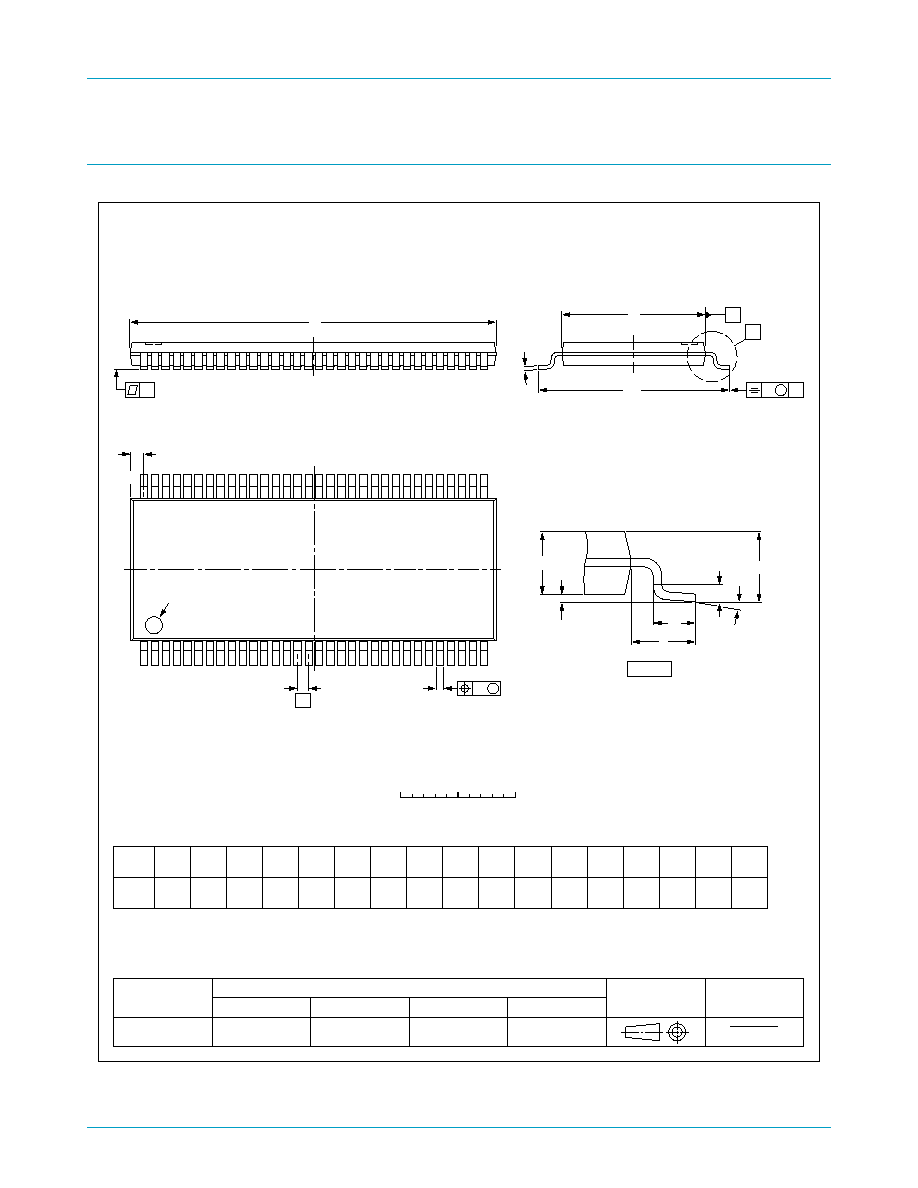
12. Package outline
Fig 17. TSSOP64 package outline (SOT646-1).
UNIT
A
1
A
2
A
3
b
p
c
D
(1)
E
(2)
e
H
E
L
L
p
Z
y
w
v
REFERENCES
OUTLINE
VERSION
EUROPEAN
PROJECTION
ISSUE DATE
IEC
JEDEC
JEITA
mm
0.15
0.05
0.2
0.1
8
0
o
o
0.1
DIMENSIONS (mm are the original dimensions).
Notes
1. Plastic or metal protrusions of 0.15 mm maximum per side are not included.
2. Plastic interlead protrusions of 0.25 mm maximum per side are not included.
SOT646-1
00-08-21
03-02-18
w
M
A
A
1
A
2
D
L
p
detail X
E
Z
e
c
L
X
(A )
3
0.25
y
bp
HE
1.05
0.85
0.27
0.17
0.2
0.1
17.1
16.9
6.2
6.0
0.5
1
0.2
8.3
7.9
0.89
0.61
0.08
0.75
0.45
v
M
A
A
TSSOP64: plastic thin shrink small outline package; 64 leads; body width 6.1 mm
SOT646-1
A
max.
1.2
0
2.5
5 mm
scale
1
64
pin 1 index
32
33
MO-153

Philips Semiconductors
GTL1655
16-bit LVTTL-to-GTL/GTL+ bus transceiver with live insertion
Product data
Rev. 01 -- 11 May 2004
19 of 23
9397 750 12936
� Koninklijke Philips Electronics N.V. 2004. All rights reserved.
13. Soldering
13.1 Introduction to soldering surface mount packages
This text gives a very brief insight to a complex technology. A more in-depth account
of soldering ICs can be found in our
Data Handbook IC26; Integrated Circuit
Packages (document order number 9398 652 90011).
There is no soldering method that is ideal for all surface mount IC packages. Wave
soldering can still be used for certain surface mount ICs, but it is not suitable for fine
pitch SMDs. In these situations reflow soldering is recommended. In these situations
reflow soldering is recommended.
13.2 Reflow soldering
Reflow soldering requires solder paste (a suspension of fine solder particles, flux and
binding agent) to be applied to the printed-circuit board by screen printing, stencilling
or pressure-syringe dispensing before package placement. Driven by legislation and
environmental forces the worldwide use of lead-free solder pastes is increasing.
Several methods exist for reflowing; for example, convection or convection/infrared
heating in a conveyor type oven. Throughput times (preheating, soldering and
cooling) vary between 100 and 200 seconds depending on heating method.
Typical reflow peak temperatures range from 215 to 270
�
C depending on solder
paste material. The top-surface temperature of the packages should preferably be
kept:
�
below 225
�
C (SnPb process) or below 245
�
C (Pb-free process)
� for all BGA, HTSSON..T and SSOP..T packages
� for packages with a thickness
2.5 mm
� for packages with a thickness < 2.5 mm and a volume
350 mm
3
so called
thick/large packages.
�
below 240
�
C (SnPb process) or below 260
�
C (Pb-free process) for packages with
a thickness < 2.5 mm and a volume < 350 mm
3
so called small/thin packages.
Moisture sensitivity precautions, as indicated on packing, must be respected at all
times.
13.3 Wave soldering
Conventional single wave soldering is not recommended for surface mount devices
(SMDs) or printed-circuit boards with a high component density, as solder bridging
and non-wetting can present major problems.
To overcome these problems the double-wave soldering method was specifically
developed.
If wave soldering is used the following conditions must be observed for optimal
results:
�
Use a double-wave soldering method comprising a turbulent wave with high
upward pressure followed by a smooth laminar wave.

Philips Semiconductors
GTL1655
16-bit LVTTL-to-GTL/GTL+ bus transceiver with live insertion
Product data
Rev. 01 -- 11 May 2004
20 of 23
9397 750 12936
� Koninklijke Philips Electronics N.V. 2004. All rights reserved.
�
For packages with leads on two sides and a pitch (e):
� larger than or equal to 1.27 mm, the footprint longitudinal axis is preferred to be
parallel to the transport direction of the printed-circuit board;
� smaller than 1.27 mm, the footprint longitudinal axis must be parallel to the
transport direction of the printed-circuit board.
The footprint must incorporate solder thieves at the downstream end.
�
For packages with leads on four sides, the footprint must be placed at a 45
�
angle
to the transport direction of the printed-circuit board. The footprint must
incorporate solder thieves downstream and at the side corners.
During placement and before soldering, the package must be fixed with a droplet of
adhesive. The adhesive can be applied by screen printing, pin transfer or syringe
dispensing. The package can be soldered after the adhesive is cured.
Typical dwell time of the leads in the wave ranges from 3 to 4 seconds at 250
�
C or
265
�
C, depending on solder material applied, SnPb or Pb-free respectively.
A mildly-activated flux will eliminate the need for removal of corrosive residues in
most applications.
13.4 Manual soldering
Fix the component by first soldering two diagonally-opposite end leads. Use a low
voltage (24 V or less) soldering iron applied to the flat part of the lead. Contact time
must be limited to 10 seconds at up to 300
�
C.
When using a dedicated tool, all other leads can be soldered in one operation within
2 to 5 seconds between 270 and 320
�
C.
13.5 Package related soldering information
[1]
For more detailed information on the BGA packages refer to the
(LF)BGA Application Note
(AN01026); order a copy from your Philips Semiconductors sales office.
[2]
All surface mount (SMD) packages are moisture sensitive. Depending upon the moisture content, the
maximum temperature (with respect to time) and body size of the package, there is a risk that internal
or external package cracks may occur due to vaporization of the moisture in them (the so called
popcorn effect). For details, refer to the Drypack information in the
Data Handbook IC26; Integrated
Circuit Packages; Section: Packing Methods.
Table 18:
Suitability of surface mount IC packages for wave and reflow soldering
methods
Package
[1]
Soldering method
Wave
Reflow
[2]
BGA, HTSSON..T
[3]
, LBGA, LFBGA, SQFP,
SSOP..T
[3]
, TFBGA, USON, VFBGA
not suitable
suitable
DHVQFN, HBCC, HBGA, HLQFP, HSO, HSOP,
HSQFP, HSSON, HTQFP, HTSSOP, HVQFN,
HVSON, SMS
not suitable
[4]
suitable
PLCC
[5]
, SO, SOJ
suitable
suitable
LQFP, QFP, TQFP
not recommended
[5][6]
suitable
SSOP, TSSOP, VSO, VSSOP
not recommended
[7]
suitable
CWQCCN..L
[8]
, PMFP
[9]
, WQCCN..L
[8]
not suitable
not suitable

Philips Semiconductors
GTL1655
16-bit LVTTL-to-GTL/GTL+ bus transceiver with live insertion
Product data
Rev. 01 -- 11 May 2004
21 of 23
9397 750 12936
� Koninklijke Philips Electronics N.V. 2004. All rights reserved.
[3]
These transparent plastic packages are extremely sensitive to reflow soldering conditions and must
on no account be processed through more than one soldering cycle or subjected to infrared reflow
soldering with peak temperature exceeding 217
�
C
�
10
�
C measured in the atmosphere of the reflow
oven. The package body peak temperature must be kept as low as possible.
[4]
These packages are not suitable for wave soldering. On versions with the heatsink on the bottom
side, the solder cannot penetrate between the printed-circuit board and the heatsink. On versions with
the heatsink on the top side, the solder might be deposited on the heatsink surface.
[5]
If wave soldering is considered, then the package must be placed at a 45
�
angle to the solder wave
direction. The package footprint must incorporate solder thieves downstream and at the side corners.
[6]
Wave soldering is suitable for LQFP, QFP and TQFP packages with a pitch (e) larger than 0.8 mm; it
is definitely not suitable for packages with a pitch (e) equal to or smaller than 0.65 mm.
[7]
Wave soldering is suitable for SSOP, TSSOP, VSO and VSOP packages with a pitch (e) equal to or
larger than 0.65 mm; it is definitely not suitable for packages with a pitch (e) equal to or smaller than
0.5 mm.
[8]
Image sensor packages in principle should not be soldered. They are mounted in sockets or delivered
pre-mounted on flex foil. However, the image sensor package can be mounted by the client on a flex
foil by using a hot bar soldering process. The appropriate soldering profile can be provided on
request.
[9]
Hot bar soldering or manual soldering is suitable for PMFP packages.
14. Revision history
Table 19:
Revision history
Rev Date
CPCN
Description
01
20040511
-
Product data (9397 750 12936).

9397 750 12936
Philips Semiconductors
GTL1655
16-bit LVTTL-to-GTL/GTL+ bus transceiver with live insertion
� Koninklijke Philips Electronics N.V. 2004. All rights reserved.
Product data
Rev. 01 -- 11 May 2004
22 of 23
Contact information
For additional information, please visit http://www.semiconductors.philips.com.
For sales office addresses, send e-mail to: sales.addresses@www.semiconductors.philips.com.
Fax: +31 40 27 24825
15. Data sheet status
[1]
Please consult the most recently issued data sheet before initiating or completing a design.
[2]
The product status of the device(s) described in this data sheet may have changed since this data sheet was published. The latest information is available on the Internet at
URL http://www.semiconductors.philips.com.
[3]
For data sheets describing multiple type numbers, the highest-level product status determines the data sheet status.
16. Definitions
Short-form specification -- The data in a short-form specification is
extracted from a full data sheet with the same type number and title. For
detailed information see the relevant data sheet or data handbook.
Limiting values definition -- Limiting values given are in accordance with
the Absolute Maximum Rating System (IEC 60134). Stress above one or
more of the limiting values may cause permanent damage to the device.
These are stress ratings only and operation of the device at these or at any
other conditions above those given in the Characteristics sections of the
specification is not implied. Exposure to limiting values for extended periods
may affect device reliability.
Application information -- Applications that are described herein for any
of these products are for illustrative purposes only. Philips Semiconductors
make no representation or warranty that such applications will be suitable for
the specified use without further testing or modification.
17. Disclaimers
Life support -- These products are not designed for use in life support
appliances, devices, or systems where malfunction of these products can
reasonably be expected to result in personal injury. Philips Semiconductors
customers using or selling these products for use in such applications do so
at their own risk and agree to fully indemnify Philips Semiconductors for any
damages resulting from such application.
Right to make changes -- Philips Semiconductors reserves the right to
make changes in the products - including circuits, standard cells, and/or
software - described or contained herein in order to improve design and/or
performance. When the product is in full production (status `Production'),
relevant changes will be communicated via a Customer Product/Process
Change Notification (CPCN). Philips Semiconductors assumes no
responsibility or liability for the use of any of these products, conveys no
licence or title under any patent, copyright, or mask work right to these
products, and makes no representations or warranties that these products are
free from patent, copyright, or mask work right infringement, unless otherwise
specified.
Level
Data sheet status
[1]
Product status
[2][3]
Definition
I
Objective data
Development
This data sheet contains data from the objective specification for product development. Philips
Semiconductors reserves the right to change the specification in any manner without notice.
II
Preliminary data
Qualification
This data sheet contains data from the preliminary specification. Supplementary data will be published
at a later date. Philips Semiconductors reserves the right to change the specification without notice, in
order to improve the design and supply the best possible product.
III
Product data
Production
This data sheet contains data from the product specification. Philips Semiconductors reserves the
right to make changes at any time in order to improve the design, manufacturing and supply. Relevant
changes will be communicated via a Customer Product/Process Change Notification (CPCN).

� Koninklijke Philips Electronics N.V. 2004.
Printed in the U.S.A.
All rights are reserved. Reproduction in whole or in part is prohibited without the prior
written consent of the copyright owner.
The information presented in this document does not form part of any quotation or
contract, is believed to be accurate and reliable and may be changed without notice. No
liability will be accepted by the publisher for any consequence of its use. Publication
thereof does not convey nor imply any license under patent- or other industrial or
intellectual property rights.
Date of release: 11 May 2004
Document order number: 9397 750 12936
Contents
Philips Semiconductors
GTL1655
16-bit LVTTL-to-GTL/GTL+ bus transceiver with live insertion
1
Description . . . . . . . . . . . . . . . . . . . . . . . . . . . . . 1
2
Features . . . . . . . . . . . . . . . . . . . . . . . . . . . . . . . 2
3
Quick reference data . . . . . . . . . . . . . . . . . . . . . 2
4
Ordering information . . . . . . . . . . . . . . . . . . . . . 3
4.1
Ordering options . . . . . . . . . . . . . . . . . . . . . . . . 3
5
Pinning information . . . . . . . . . . . . . . . . . . . . . . 4
5.1
Pinning . . . . . . . . . . . . . . . . . . . . . . . . . . . . . . . 4
5.2
Pin description . . . . . . . . . . . . . . . . . . . . . . . . . 5
6
Functional description . . . . . . . . . . . . . . . . . . . 6
6.1
Function table . . . . . . . . . . . . . . . . . . . . . . . . . . 7
7
Limiting values. . . . . . . . . . . . . . . . . . . . . . . . . . 8
8
Recommended operating conditions. . . . . . . . 9
9
Static characteristics. . . . . . . . . . . . . . . . . . . . 10
10
Dynamic characteristics . . . . . . . . . . . . . . . . . 12
10.1
AC waveforms. . . . . . . . . . . . . . . . . . . . . . . . . 15
11
Test information . . . . . . . . . . . . . . . . . . . . . . . . 17
12
Package outline . . . . . . . . . . . . . . . . . . . . . . . . 18
13
Soldering . . . . . . . . . . . . . . . . . . . . . . . . . . . . . 19
13.1
Introduction to soldering surface mount
packages . . . . . . . . . . . . . . . . . . . . . . . . . . . . 19
13.2
Reflow soldering . . . . . . . . . . . . . . . . . . . . . . . 19
13.3
Wave soldering . . . . . . . . . . . . . . . . . . . . . . . . 19
13.4
Manual soldering . . . . . . . . . . . . . . . . . . . . . . 20
13.5
Package related soldering information . . . . . . 20
14
Revision history . . . . . . . . . . . . . . . . . . . . . . . . 21
15
Data sheet status . . . . . . . . . . . . . . . . . . . . . . . 22
16
Definitions . . . . . . . . . . . . . . . . . . . . . . . . . . . . 22
17
Disclaimers . . . . . . . . . . . . . . . . . . . . . . . . . . . . 22
Document Outline