GTL2009
3-bit GTL Front-Side Bus frequency comparator

1.
General description
The GTL2009 is designed for the Nocona and Dempsey/Blackford dual Intel Xeon
processor platforms to compare the Front-Side Bus (FSB) frequency settings and set the
common FSB frequency at the lowest setting if both processor slots are occupied or the
FSB setting of the occupied processor slot if only one processor is being used. A default
FSB frequency of 100 MHz is initially set upon power-up when V
DD
is greater than 1.5 V.
Magnitude comparisons and frequency multiplexing to compute the common FSB
frequency occurs when the two 3-bit FSB GTL inputs from the chip sets are valid. The
common FSB frequency GTL outputs switch from the default frequency to the computed
frequency when the GTL reference voltage input (VREF) crosses a static 0.6 V internally
generated input comparator reference voltage. The GTL2009 then continually monitors
the FSB frequency and slot occupied inputs for any further changes.
The Nocona and Dempsey/Blackford Xeon processors specify a V
TT
of 1.2 V and 1.1 V,
as well as a nominal V
ref
of 0.76 V and 0.73 V respectively. To allow for future voltage level
changes that may extend V
ref
to 0.63 of V
TT
(minimum of 0.693 V with V
TT
of 1.1 V) the
GTL2009 allows a minimum V
ref
of 0.66 V. Characterization results show that there is little
DC or AC performance variation between these levels.
The GTL2009 is a companion chip to the GTL2006 platform health management
GTL-to-LVTTL translator and the newer GTL2007 that adds an enable function that
disables the error output to the monitoring agent for platforms that monitor the individual
error conditions from each processor.
2.
Features
s
Compares FSB frequency inputs to set the lowest frequency as the common bus
frequency.
s
Operates at a range of GTL signal levels
s
3.0 V to 3.6 V operation
s
LVTTL I/O are not 5 V tolerant
s
Companion chip to GTL2006 and GTL2007
s
ESD protection exceeds 2000 V HBM per JESD22-A114, 200 V MM per
JESD22-A115 and 1000 V CDM per JESD22-C101
s
Latch-up testing is done to JEDEC Standard JESD78, which exceeds 500 mA
s
Available in TSSOP16 package
GTL2009
3-bit GTL Front-Side Bus frequency comparator
Rev. 01 -- 22 September 2005
Product data sheet
9397 750 13556
� Koninklijke Philips Electronics N.V. 2005. All rights reserved.
Product data sheet
Rev. 01 -- 22 September 2005
2 of 17
Philips Semiconductors
GTL2009
3-bit GTL Front-Side Bus frequency comparator
3.
Quick reference data
4.
Ordering information
5.
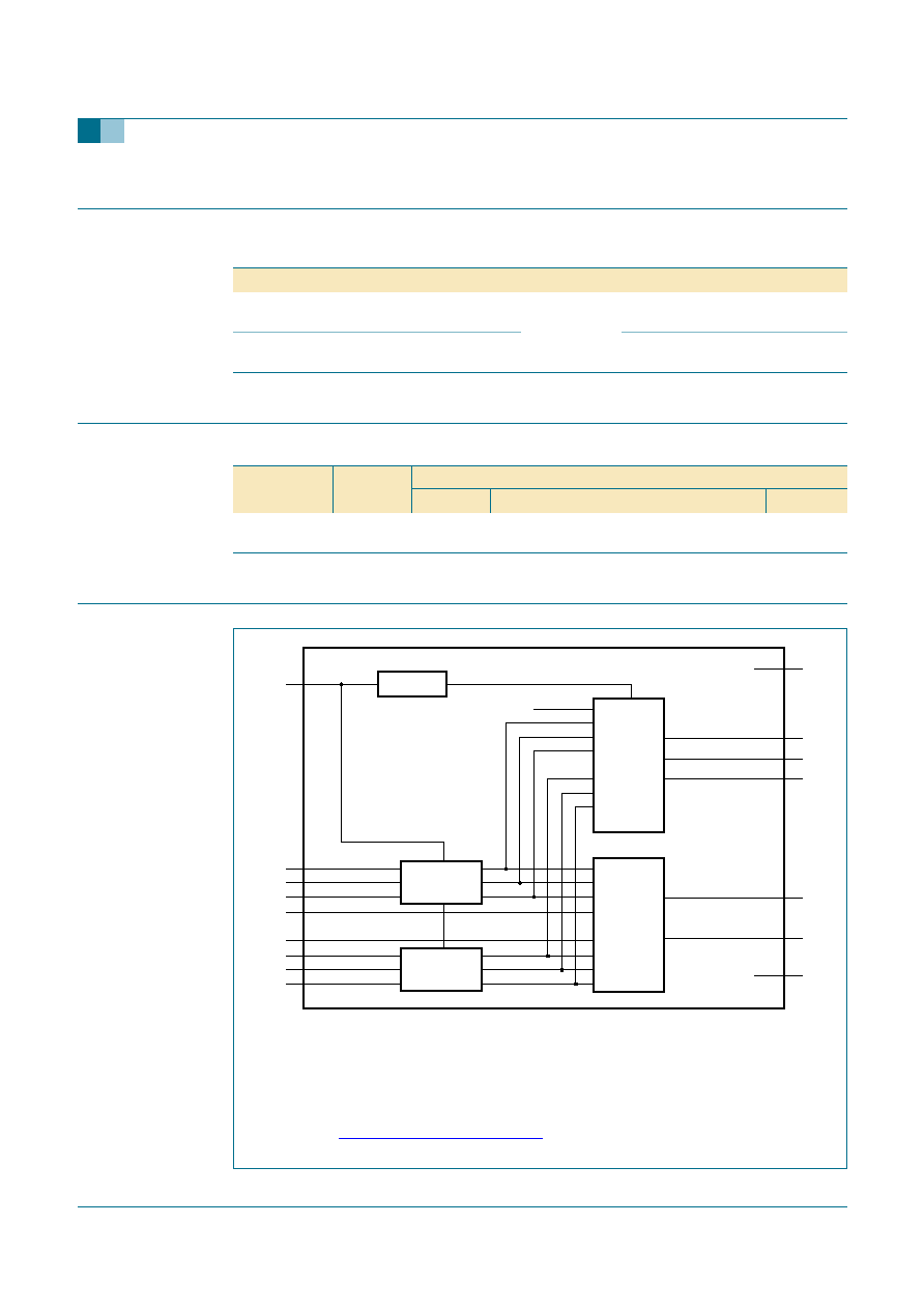
Functional diagram
Table 1:
Quick reference data
T
amb
= 25
�
C
Symbol
Parameter
Conditions
Min
Typ
Max
Unit
t
PLH
LOW-to-HIGH propagation delay;
BI to BO
C
L
= 30 pF;
V
DD
= 3.3 V
3.0
16.5
30
ns
t
PHL
HIGH-to-LOW propagation delay;
BI to BO
2.3
16.2
30
ns
Table 2:
Ordering information
Type number
Topside
mark
Package
Name
Description
Version
GTL2009PW
GTL2009
TSSOP16
plastic thin shrink small outline package;
16 leads; body width 4.4 mm
SOT403-1
If B - Occupied only, then A
B = 1.
If A - Occupied only, then A
B = 0.
If A and B - Occupied, then A
B = 1 if A frequency higher than B frequency.
Pin assignment: A = LVTTL, B = GTL, I = Input, O = Output.
Refer to
Section 7.2 "Default conditions input"
.
Fig 1.
Functional diagram of GTL2009
GTL2009
002aaa997
BO1
BO2
BO3
common
FSB
MUX
BSEL1
BSEL2
BSEL3
default output is
101 = 100 MHz
COMPARE
A
B
equal
AO2
AO1
V
SS
A
B
A
B
1 = B
VREF
V
DD
GTL to TTL
A
B
B - BSEL1
B - BSEL2
B - BSEL3
2BI1
2BI2
2BI3
GTL to TTL
A - Occupied#
active LOW
A - BSEL1
A - BSEL2
A - BSEL3
1AI
1BI1
1BI2
1BI3
B - Occupied#
active LOW
2AI
START-UP
9397 750 13556
� Koninklijke Philips Electronics N.V. 2005. All rights reserved.
Product data sheet
Rev. 01 -- 22 September 2005
3 of 17
Philips Semiconductors
GTL2009
3-bit GTL Front-Side Bus frequency comparator
6.
Pinning information
6.1 Pinning
6.2 Pin description
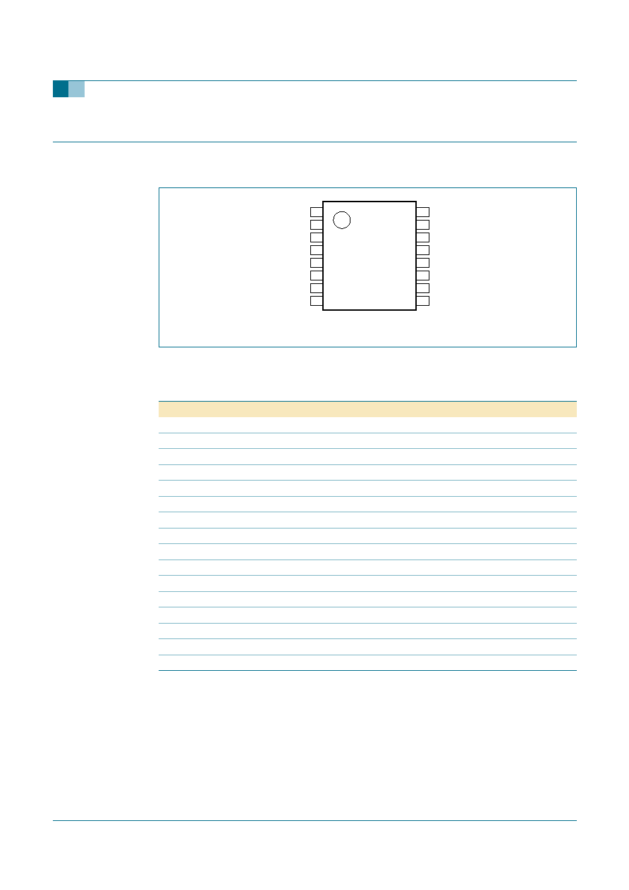
Fig 2.
Pin configuration for TSSOP16
GTL2009PW
V
DD
1BI1
VREF
1BI2
BO3
1BI3
BO2
1AI
BO1
2AI
AO2
2BI1
AO1
2BI2
V
SS
2BI3
002aaa996
1
2
3
4
5
6
7
8
10
9
12
11
14
13
16
15
Table 3:
Pin description
Symbol
Pin
Type
Description
V
DD
1
supply
supply voltage
VREF
2
V
ref
V
ref
input voltage
BO3
3
GTL output
BSEL3
BO2
4
GTL output
BSEL2
BO1
5
GTL output
BSEL1
AO2
6
LVTTL output
A
B
AO1
7
LVTTL output
equal
V
SS
8
ground
ground supply
2BI3
9
GTL input
B-BSEL3
2BI2
10
GTL input
B-BSEL2
2BI1
11
GTL input
B-BSEL1
2AI
12
LVTTL input
B-occupied
1AI
13
LVTTL input
A-occupied
1BI3
14
GTL input
A-BSEL3
1BI2
15
GTL input
A-BSEL2
1BI1
16
GTL input
A-BSEL1

9397 750 13556
� Koninklijke Philips Electronics N.V. 2005. All rights reserved.
Product data sheet
Rev. 01 -- 22 September 2005
4 of 17
Philips Semiconductors
GTL2009
3-bit GTL Front-Side Bus frequency comparator
7.
Functional description
Refer to
Figure 1 "Functional diagram of GTL2009"
.
7.1 Function tables
Table 4:
FSB frequency selection
BSEL3
BSEL2
BSEL1
FSB
H
L
H
100 MHz
L
L
H
133 MHz
L
H
H
166 MHz
L
H
L
200 MHz
L
L
L
266 MHz
H
L
L
333 MHz
H
H
L
400 MHz
H
H
H
reserved
Table 5:
FSB frequency comparison
Default on start-up is 101
Processor A FSB
Processor B FSB
Pins BO1/BO2/BO3
Common FSB frequency
A
B
A
B
B
A < B
A < B
A
not occupied
B
B
A
not occupied
A
A = B
A = B
A or B
Table 6:
FSB the same output
Processor A FSB
Processor B FSB
Compare
Pin AO1
A frequency = B frequency
A > B
A > B
no
L
A < B
A < B
no
L
A = B
A = B
yes
H
Table 7:
FSB processor A greater than or equal to processor B output
Pin 1AI
Pin 2AI
Compare
Pin AO2
A-occupied
B-occupied
A frequency > B frequency
L
yes
L
yes
no
L
yes
H
H
no
L
yes
X
H
L
yes
H
no
X
L
H
no
H
no
X
H

9397 750 13556
� Koninklijke Philips Electronics N.V. 2005. All rights reserved.
Product data sheet
Rev. 01 -- 22 September 2005
5 of 17
Philips Semiconductors
GTL2009
3-bit GTL Front-Side Bus frequency comparator
7.2 Default conditions input
The FSB GTL output data is masked and a specific default value (100 MHz) is inserted
upon power-up when V
DD
is greater than 1.5 V. The FSB GTL output data is unmasked
and valid data is supplied when the VREF input crosses a static 0.6 V internally generated
input comparator reference voltage. For slowly rising GTL V
TT
supply (0.7 V/500
�
s), the
switch-over happens at the 0.6 V threshold. For fast rising GTL V
TT
supply (0.7 V/100 ns),
the switch-over typically occurs between 350 ns to 1.5
�
s after the 0.6 V threshold is
exceeded.
The AO1 and AO2 outputs do not have `default conditions' like those assigned to the GTL
outputs. Instead, these two pins will power-up according to the conditions applied to the
1A1 and 2A1 input pins as shown in
Table 8
. If the slot is occupied, the input is LOW.
It is important to note that the AO1 and AO2 outputs may be valid a little before 1.5 V and
will rise with V
DD
. Valid outputs from the system level perspective will be achieved after
V
DD
is in regulation, V
TT
ramps up, and after the internal propagation delay of the
GTL2009. No firm answer for this can be given since the time it takes for V
DD
to be in
regulation varies from 100 ms to 1000 ms, and the rise time of V
TT
is unknown. The
GTL2009 outputs are valid after the GTL inputs are valid plus 19.6 ns (worst-case
propagation delay of the GTL-to-LVTTL path).
Table 8:
AO1 and AO2 power-up conditions
H = HIGH; L = LOW.
1AI
2AI
V
DD
AO1
AO2
L
L
<1.5 V
L
L
L
L
>1.5 V
H
H
L
H
<1.5 V
L
L
L
H
>1.5 V
L
L
H
L
<1.5 V
L
L
H
L
>1.5 V
L
H
H
H
<1.5 V
L
L
H
H
>1.5 V
H
H
9397 750 13556
� Koninklijke Philips Electronics N.V. 2005. All rights reserved.
Product data sheet
Rev. 01 -- 22 September 2005
6 of 17
Philips Semiconductors
GTL2009
3-bit GTL Front-Side Bus frequency comparator
8.
Application design-in information
8.1 Frequently asked questions
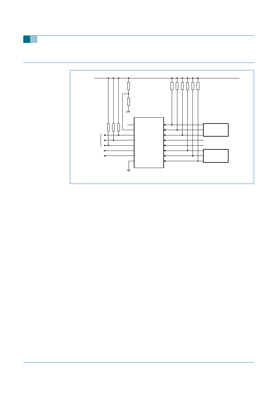
Question 1: When the GTL2009 is unpowered, the LVTTL inputs may be pulled up to
3.3 V and we want to make sure that there is no leakage path to the power rail under this
condition. Are the LVTTL inputs high-impedance when the device is unpowered and will
there be any leakage?
Answer 1: When the device is unpowered, the LVTTL inputs will be in a high-impedance
state and will not leak to V
DD
if they are pulled HIGH or LOW while the device is
unpowered.
Question 2: What is the condition of the GTL and LVTTL output pins when the device is
unpowered?
Answer 2: The open-drain GTL outputs will not leak to the power supply if they are pulled
HIGH or allowed to float while the device is unpowered. The GTL inputs will also not leak
to the power supply under the same conditions. The LVTTL totem pole outputs, however,
are not open-drain type outputs and there will be current flow on these pins if they are
pulled HIGH when V
DD
is at ground.
Fig 3.
Application diagram
002aaa998
V
TT
V
TT
56
R
2R
V
DD
VREF
BO3
BO2
BO1
AO2
AO1
V
SS
1BI1
1BI2
1BI3
2AI
2BI1
2BI2
2BI3
common
front-side bus
PROCESSOR
A
PROCESSOR
B
slot B occupied
1AI
slot A occupied

9397 750 13556
� Koninklijke Philips Electronics N.V. 2005. All rights reserved.
Product data sheet
Rev. 01 -- 22 September 2005
7 of 17
Philips Semiconductors
GTL2009
3-bit GTL Front-Side Bus frequency comparator
9.
Limiting values
[1]
Stresses beyond those listed may cause permanent damage to the device. These are stress ratings only and functional operation of the
device at these or any other conditions beyond those indicated under
Section 10 "Recommended operating conditions"
is not implied.
Exposure to absolute-maximum-rated conditions for extended periods may affect device reliability.
[2]
The performance capability of a high-performance integrated circuit in conjunction with its thermal environment can create junction
temperatures which are detrimental to reliability. The maximum junction temperature of this integrated circuit should not exceed 150
�
C.
[3]
The input and output negative voltage ratings may be exceeded if the input and output clamp current ratings are observed.
[4]
Current into any output in the LOW state.
[5]
Current into any output in the HIGH state.
10. Recommended operating conditions
Table 9:
Limiting values
In accordance with the Absolute Maximum Rating System (IEC 60134).
[1]
Voltages are referenced to V
SS
(ground = 0 V).
Symbol
Parameter
Conditions
Min
Max
Unit
V
DD
supply voltage
-
0.5
+4.6
V
I
IK
input clamping current
V
I
< 0 V
-
-
50
mA
V
I
input voltage
A port (LVTTL)
[3]
-
0.5
+4.6
V
B port (GTL)
[3]
-
-
50
mA
I
OK
output clamping current
V
O
< 0 V
-
-
50
mA
V
O
output voltage
output in Off or HIGH state; A port
[3]
-
0.5
+4.6
V
output in Off or HIGH state; B port
[3]
-
0.5
+4.6
V
I
OL
LOW-state output current
[4]
A port
-
24
mA
B port
-
30
mA
I
OH
HIGH-state output current
[5]
A port
-
-
24
mA
T
stg
storage temperature
-
60
+150
�
C
T
j
junction temperature
[2]
-
+125
�
C
Table 10:
Recommended operating conditions
Symbol
Parameter
Conditions
Min
Typ
Max
Unit
V
DD
supply voltage
3.0
3.3
3.6
V
V
TT
termination voltage
GTL
-
1.2
-
V
V
ref
reference voltage
GTL
0.66
0.8
1.1
V
V
I
input voltage
A port
0
3.3
3.6
V
B port
0
V
TT
3.6
V
V
IH
HIGH-state input voltage
A port
2
-
-
V
B port
V
ref
+ 0.050
-
-
V
V
IL
LOW-state input voltage
A port
-
-
0.8
V
B port
-
-
V
ref
-
0.050
V
I
OH
HIGH-state output current
A port
-
-
�12
mA
I
OL
LOW-state output current
A port
-
-
12
mA
B port
-
-
15
mA
T
amb
ambient temperature
operating in free air
-
40
-
+85
�
C

9397 750 13556
� Koninklijke Philips Electronics N.V. 2005. All rights reserved.
Product data sheet
Rev. 01 -- 22 September 2005
8 of 17
Philips Semiconductors
GTL2009
3-bit GTL Front-Side Bus frequency comparator
11. Static characteristics
[1]
All typical values are measured at V
DD
= 3.3 V and T
amb
= 25
�
C.
[2]
The input and output voltage ratings may be exceeded if the input and output current ratings are observed.
[3]
This is the increase in supply current for each input that is at the specified LVTTL voltage level, rather than V
DD
or V
SS
.
Table 11:
Static characteristics
Over recommended operating conditions. Voltages are referenced to V
SS
(ground = 0 V). T
amb
=
-
40
�
C to +85
�
C.
Symbol
Parameter
Conditions
Min
Typ
[1]
Max
Unit
V
OH
HIGH-level output voltage; A port
V
DD
= 3.0 V to 3.6 V;
I
OH
=
-
100
�
A
[2]
V
DD
-
0.2
2.99
-
V
V
DD
= 3.0 V; I
OH
=
-
16 mA
[2]
2.1
2.37
-
V
V
OL
LOW-level output voltage; A port
V
DD
= 3.0 V; I
OL
= 8 mA
[2]
-
0.27
0.4
V
V
DD
= 3.0 V; I
OL
= 12 mA
[2]
-
0.4
0.55
V
LOW-level output voltage; B port
V
DD
= 3.0 V; I
OL
= 15 mA
[2]
-
0.11
0.4
V
I
I
input current; A port
V
DD
= 3.6 V; V
I
= V
DD
-
-
�
1
�
A
V
DD
= 3.6 V; V
I
= 0 V
-
-
�
1
�
A
input current; B port
V
DD
= 3.6 V; V
I
= V
TT
or V
SS
-
-
�
1
�
A
I
LO
output leakage current; B port
V
DD
= 3.6 V; V
O
= V
TT
-
-
�
1
�
A
I
DD
supply current; A or B port
V
DD
= 3.6 V; V
I
= V
DD
or V
SS
;
I
O
= 0 mA
-
5.5
10
mA
I
DD
additional quiescent supply current;
A port or control inputs
V
DD
= 3.6 V; V
I
= V
DD
-
0.6 V
[3]
-
32
500
�
A
C
io
input/output capacitance; A port
V
O
= 3.0 V or 0 V
-
7.8
-
pF
input/output capacitance; B port
V
O
= V
TT
or 0 V
-
4.5
-
pF
9397 750 13556
� Koninklijke Philips Electronics N.V. 2005. All rights reserved.
Product data sheet
Rev. 01 -- 22 September 2005
9 of 17
Philips Semiconductors
GTL2009
3-bit GTL Front-Side Bus frequency comparator
12. Dynamic characteristics
[1]
All typical values are at V
DD
= 3.3 V and T
amb
= 25
�
C.
Table 12:
Dynamic characteristics
V
DD
= 3.3 V
�
0.3 V
Symbol
Parameter
Conditions
Limits
Unit
V
ref
= 0.73 V;
V
TT
= 1.1 V
V
ref
= 0.76 V;
V
TT
= 1.2 V
Min
Typ
[1]
Max
Min
Typ
[1]
Max
t
PLH
LOW-to-HIGH propagation delay; AI to AO
Figure 4
and
Figure 8
1.4
7.9
14.5
1.4
7.8
14.5
ns
t
PHL
HIGH-to-LOW propagation delay; AI to AO
2.0
9.0
16.0
2.0
8.8
16.0
ns
t
PLH
LOW-to-HIGH propagation delay; BI to AO
Figure 6
2.6
16.3
30.0
2.5
16.5
30.5
ns
t
PHL
HIGH-to-LOW propagation delay; BI to AO
2.8
13.9
25.0
2.9
14.0
25.0
ns
t
PLH
LOW-to-HIGH propagation delay; BI to BO
Figure 7
3.0
16.5
30.0
3.0
16.5
30.0
ns
t
PHL
HIGH-to-LOW propagation delay; BI to
BO
2.3
16.2
30.0
2.3
16.2
30.0
ns
t
PLH
LOW-to-HIGH propagation delay; AI to BO
Figure 5
2.1
7.9
14.0
2.0
8.3
14.5
ns
t
PHL
HIGH-to-LOW propagation delay; AI to
BO
1.4
7.3
13.5
1.5
7.7
14.0
ns
9397 750 13556
� Koninklijke Philips Electronics N.V. 2005. All rights reserved.
Product data sheet
Rev. 01 -- 22 September 2005
10 of 17
Philips Semiconductors
GTL2009
3-bit GTL Front-Side Bus frequency comparator
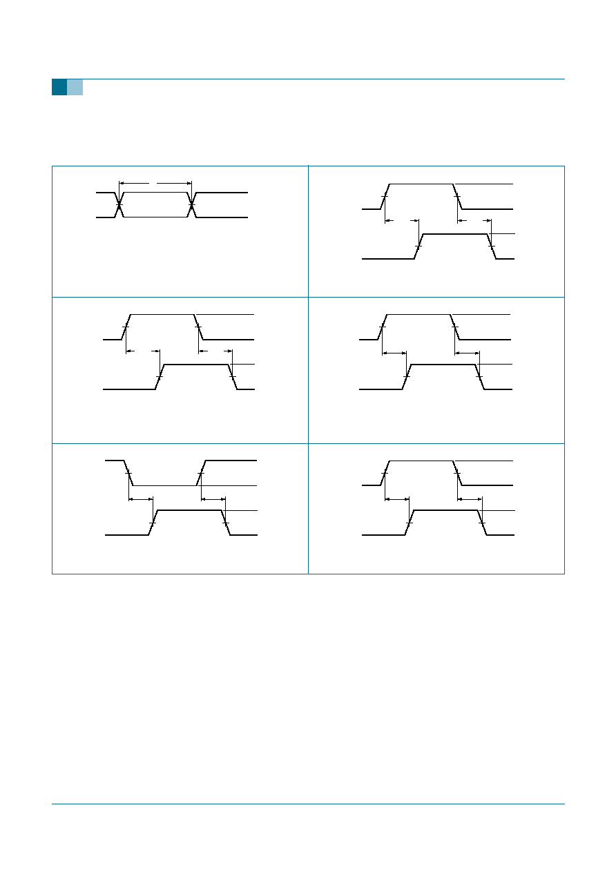
12.1 AC waveforms
V
M
= 1.5 V at V
DD
3.0 V for A ports; V
M
= V
ref
for B ports.
V
M
= 1.5 V for A port and V
ref
for B port.
V
OH
= 3 V for A port and V
TT
for B port
t
p
= pulse duration
Fig 4.
Pulse duration
Fig 5.
Propagation delay, A port to B port
PRR
10 MHz; Z
o
= 50
; t
r
2.5 ns; t
f
2.5 ns
Fig 6.
Propagation delay, BI to AO
Fig 7.
Propagation delay, BI to BO
Fig 8.
Propagation delay, AI to AO
Fig 9.
Propagation delay, 1AI to AO2
002aaa999
V
OH
0 V
t
p
V
M
V
M
002aab000
3.0 V
0 V
V
TT
V
OL
t
PLH
t
PHL
V
ref
V
ref
1.5 V
1.5 V
input
output
002aab001
V
TT
1
/
3
V
TT
V
OH
V
OL
t
PLH
t
PHL
1.5 V
1.5 V
V
ref
V
ref
input
output
002aab003
V
TT
1
/
3
V
TT
V
TT
V
OL
t
PLH
t
PHL
V
ref
V
ref
input
output
V
ref
V
ref
002aab004
3.0 V
0 V
V
OH
V
OL
t
PLH
t
PHL
1.5 V
1.5 V
input
output
1.5 V
1.5 V
002aab664
3.0 V
0 V
V
OH
V
OL
t
PLH
t
PHL
1.5 V
1.5 V
input
output
1.5 V
1.5 V
9397 750 13556
� Koninklijke Philips Electronics N.V. 2005. All rights reserved.
Product data sheet
Rev. 01 -- 22 September 2005
11 of 17
Philips Semiconductors
GTL2009
3-bit GTL Front-Side Bus frequency comparator
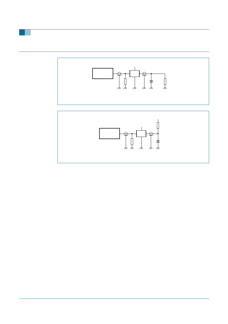
13. Test information
Definitions:
R
L
-- load resistor
C
L
-- load capacitance includes jig and probe capacitance.
R
T
-- termination resistance should be equal to Z
o
of pulse generators.
Fig 10. Load circuitry for A outputs
Fig 11. Load circuit for B outputs
PULSE
GENERATOR
V
O
CL
50 pF
002aab006
RL
500
RT
V
I
V
DD
D.U.T.
PULSE
GENERATOR
D.U.T.
VO
CL
30 pF
50
002aab007
RT
VI
V
DD
V
TT
9397 750 13556
� Koninklijke Philips Electronics N.V. 2005. All rights reserved.
Product data sheet
Rev. 01 -- 22 September 2005
12 of 17
Philips Semiconductors
GTL2009
3-bit GTL Front-Side Bus frequency comparator
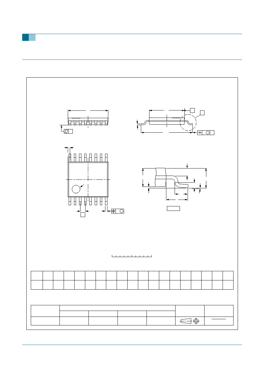
14. Package outline
Fig 12. Package outline SOT403-1 (TSSOP16)
UNIT
A
1
A
2
A
3
b
p
c
D
(1)
E
(2)
(1)
e
H
E
L
L
p
Q
Z
y
w
v
REFERENCES
OUTLINE
VERSION
EUROPEAN
PROJECTION
ISSUE DATE
IEC
JEDEC
JEITA
mm
0.15
0.05
0.95
0.80
0.30
0.19
0.2
0.1
5.1
4.9
4.5
4.3
0.65
6.6
6.2
0.4
0.3
0.40
0.06
8
0
o
o
0.13
0.1
0.2
1
DIMENSIONS (mm are the original dimensions)
Notes
1. Plastic or metal protrusions of 0.15 mm maximum per side are not included.
2. Plastic interlead protrusions of 0.25 mm maximum per side are not included.
0.75
0.50
SOT403-1
MO-153
99-12-27
03-02-18
w
M
b
p
D
Z
e
0.25
1
8
16
9
A
A
1
A
2
L
p
Q
detail X
L
(A )
3
H
E
E
c
v
M
A
X
A
y
0
2.5
5 mm
scale
TSSOP16: plastic thin shrink small outline package; 16 leads; body width 4.4 mm
SOT403-1
A
max.
1.1
pin 1 index

9397 750 13556
� Koninklijke Philips Electronics N.V. 2005. All rights reserved.
Product data sheet
Rev. 01 -- 22 September 2005
13 of 17
Philips Semiconductors
GTL2009
3-bit GTL Front-Side Bus frequency comparator
15. Soldering
15.1 Introduction to soldering surface mount packages
This text gives a very brief insight to a complex technology. A more in-depth account of
soldering ICs can be found in our
Data Handbook IC26; Integrated Circuit Packages
(document order number 9398 652 90011).
There is no soldering method that is ideal for all surface mount IC packages. Wave
soldering can still be used for certain surface mount ICs, but it is not suitable for fine pitch
SMDs. In these situations reflow soldering is recommended.
15.2 Reflow soldering
Reflow soldering requires solder paste (a suspension of fine solder particles, flux and
binding agent) to be applied to the printed-circuit board by screen printing, stencilling or
pressure-syringe dispensing before package placement. Driven by legislation and
environmental forces the worldwide use of lead-free solder pastes is increasing.
Several methods exist for reflowing; for example, convection or convection/infrared
heating in a conveyor type oven. Throughput times (preheating, soldering and cooling)
vary between 100 seconds and 200 seconds depending on heating method.
Typical reflow peak temperatures range from 215
�
C to 270
�
C depending on solder paste
material. The top-surface temperature of the packages should preferably be kept:
�
below 225
�
C (SnPb process) or below 245
�
C (Pb-free process)
� for all BGA, HTSSON..T and SSOP..T packages
� for packages with a thickness
2.5 mm
� for packages with a thickness < 2.5 mm and a volume
350 mm
3
so called
thick/large packages.
�
below 240
�
C (SnPb process) or below 260
�
C (Pb-free process) for packages with a
thickness < 2.5 mm and a volume < 350 mm
3
so called small/thin packages.
Moisture sensitivity precautions, as indicated on packing, must be respected at all times.
15.3 Wave soldering
Conventional single wave soldering is not recommended for surface mount devices
(SMDs) or printed-circuit boards with a high component density, as solder bridging and
non-wetting can present major problems.
To overcome these problems the double-wave soldering method was specifically
developed.
If wave soldering is used the following conditions must be observed for optimal results:
�
Use a double-wave soldering method comprising a turbulent wave with high upward
pressure followed by a smooth laminar wave.
�
For packages with leads on two sides and a pitch (e):
� larger than or equal to 1.27 mm, the footprint longitudinal axis is preferred to be
parallel to the transport direction of the printed-circuit board;
9397 750 13556
� Koninklijke Philips Electronics N.V. 2005. All rights reserved.
Product data sheet
Rev. 01 -- 22 September 2005
14 of 17
Philips Semiconductors
GTL2009
3-bit GTL Front-Side Bus frequency comparator
� smaller than 1.27 mm, the footprint longitudinal axis must be parallel to the
transport direction of the printed-circuit board.
The footprint must incorporate solder thieves at the downstream end.
�
For packages with leads on four sides, the footprint must be placed at a 45
�
angle to
the transport direction of the printed-circuit board. The footprint must incorporate
solder thieves downstream and at the side corners.
During placement and before soldering, the package must be fixed with a droplet of
adhesive. The adhesive can be applied by screen printing, pin transfer or syringe
dispensing. The package can be soldered after the adhesive is cured.
Typical dwell time of the leads in the wave ranges from 3 seconds to 4 seconds at 250
�
C
or 265
�
C, depending on solder material applied, SnPb or Pb-free respectively.
A mildly-activated flux will eliminate the need for removal of corrosive residues in most
applications.
15.4 Manual soldering
Fix the component by first soldering two diagonally-opposite end leads. Use a low voltage
(24 V or less) soldering iron applied to the flat part of the lead. Contact time must be
limited to 10 seconds at up to 300
�
C.
When using a dedicated tool, all other leads can be soldered in one operation within
2 seconds to 5 seconds between 270
�
C and 320
�
C.
15.5 Package related soldering information
[1]
For more detailed information on the BGA packages refer to the
(LF)BGA Application Note (AN01026);
order a copy from your Philips Semiconductors sales office.
[2]
All surface mount (SMD) packages are moisture sensitive. Depending upon the moisture content, the
maximum temperature (with respect to time) and body size of the package, there is a risk that internal or
external package cracks may occur due to vaporization of the moisture in them (the so called popcorn
effect). For details, refer to the Drypack information in the
Data Handbook IC26; Integrated Circuit
Packages; Section: Packing Methods.
[3]
These transparent plastic packages are extremely sensitive to reflow soldering conditions and must on no
account be processed through more than one soldering cycle or subjected to infrared reflow soldering with
peak temperature exceeding 217
�
C
�
10
�
C measured in the atmosphere of the reflow oven. The package
body peak temperature must be kept as low as possible.
Table 13:
Suitability of surface mount IC packages for wave and reflow soldering methods
Package
[1]
Soldering method
Wave
Reflow
[2]
BGA, HTSSON..T
[3]
, LBGA, LFBGA, SQFP,
SSOP..T
[3]
, TFBGA, VFBGA, XSON
not suitable
suitable
DHVQFN, HBCC, HBGA, HLQFP, HSO, HSOP,
HSQFP, HSSON, HTQFP, HTSSOP, HVQFN,
HVSON, SMS
not suitable
[4]
suitable
PLCC
[5]
, SO, SOJ
suitable
suitable
LQFP, QFP, TQFP
not recommended
[5] [6]
suitable
SSOP, TSSOP, VSO, VSSOP
not recommended
[7]
suitable
CWQCCN..L
[8]
, PMFP
[9]
, WQCCN..L
[8]
not suitable
not suitable

9397 750 13556
� Koninklijke Philips Electronics N.V. 2005. All rights reserved.
Product data sheet
Rev. 01 -- 22 September 2005
15 of 17
Philips Semiconductors
GTL2009
3-bit GTL Front-Side Bus frequency comparator
[4]
These packages are not suitable for wave soldering. On versions with the heatsink on the bottom side, the
solder cannot penetrate between the printed-circuit board and the heatsink. On versions with the heatsink
on the top side, the solder might be deposited on the heatsink surface.
[5]
If wave soldering is considered, then the package must be placed at a 45
�
angle to the solder wave
direction. The package footprint must incorporate solder thieves downstream and at the side corners.
[6]
Wave soldering is suitable for LQFP, QFP and TQFP packages with a pitch (e) larger than 0.8 mm; it is
definitely not suitable for packages with a pitch (e) equal to or smaller than 0.65 mm.
[7]
Wave soldering is suitable for SSOP, TSSOP, VSO and VSSOP packages with a pitch (e) equal to or larger
than 0.65 mm; it is definitely not suitable for packages with a pitch (e) equal to or smaller than 0.5 mm.
[8]
Image sensor packages in principle should not be soldered. They are mounted in sockets or delivered
pre-mounted on flex foil. However, the image sensor package can be mounted by the client on a flex foil by
using a hot bar soldering process. The appropriate soldering profile can be provided on request.
[9]
Hot bar soldering or manual soldering is suitable for PMFP packages.
16. Abbreviations
17. Revision history
Table 14:
Abbreviations
Acronym
Definition
CDM
Charged Device Model
ESD
Electrostatic Discharge
FSB
Front-Side Bus
GTL
Gunning Transceiver Logic
HBM
Human Body Model
LVTTL
Low Voltage Transistor-Transistor Logic
MM
Machine Model
PRR
Pulse Rate Repetition
Table 15:
Revision history
Document ID
Release date
Data sheet status
Change notice
Doc. number
Supersedes
GTL2009_1
20050922
Product data sheet
-
9397 750 13556
-

Philips Semiconductors
GTL2009
3-bit GTL Front-Side Bus frequency comparator
9397 750 13556
� Koninklijke Philips Electronics N.V. 2005. All rights reserved.
Product data sheet
Rev. 01 -- 22 September 2005
16 of 17
18. Data sheet status
[1]
Please consult the most recently issued data sheet before initiating or completing a design.
[2]
The product status of the device(s) described in this data sheet may have changed since this data sheet was published. The latest information is available on the Internet at
URL http://www.semiconductors.philips.com.
[3]
For data sheets describing multiple type numbers, the highest-level product status determines the data sheet status.
19. Definitions
Short-form specification -- The data in a short-form specification is
extracted from a full data sheet with the same type number and title. For
detailed information see the relevant data sheet or data handbook.
Limiting values definition -- Limiting values given are in accordance with
the Absolute Maximum Rating System (IEC 60134). Stress above one or
more of the limiting values may cause permanent damage to the device.
These are stress ratings only and operation of the device at these or at any
other conditions above those given in the Characteristics sections of the
specification is not implied. Exposure to limiting values for extended periods
may affect device reliability.
Application information -- Applications that are described herein for any
of these products are for illustrative purposes only. Philips Semiconductors
make no representation or warranty that such applications will be suitable for
the specified use without further testing or modification.
20. Disclaimers
Life support -- These products are not designed for use in life support
appliances, devices, or systems where malfunction of these products can
reasonably be expected to result in personal injury. Philips Semiconductors
customers using or selling these products for use in such applications do so
at their own risk and agree to fully indemnify Philips Semiconductors for any
damages resulting from such application.
Right to make changes -- Philips Semiconductors reserves the right to
make changes in the products - including circuits, standard cells, and/or
software - described or contained herein in order to improve design and/or
performance. When the product is in full production (status `Production'),
relevant changes will be communicated via a Customer Product/Process
Change Notification (CPCN). Philips Semiconductors assumes no
responsibility or liability for the use of any of these products, conveys no
license or title under any patent, copyright, or mask work right to these
products, and makes no representations or warranties that these products are
free from patent, copyright, or mask work right infringement, unless otherwise
specified.
21. Trademarks
Notice -- All referenced brands, product names, service names and
trademarks are the property of their respective owners.
22. Contact information
For additional information, please visit: http://www.semiconductors.philips.com
For sales office addresses, send an email to: sales.addresses@www.semiconductors.philips.com
Level
Data sheet status
[1]
Product status
[2] [3]
Definition
I
Objective data
Development
This data sheet contains data from the objective specification for product development. Philips
Semiconductors reserves the right to change the specification in any manner without notice.
II
Preliminary data
Qualification
This data sheet contains data from the preliminary specification. Supplementary data will be published
at a later date. Philips Semiconductors reserves the right to change the specification without notice, in
order to improve the design and supply the best possible product.
III
Product data
Production
This data sheet contains data from the product specification. Philips Semiconductors reserves the
right to make changes at any time in order to improve the design, manufacturing and supply. Relevant
changes will be communicated via a Customer Product/Process Change Notification (CPCN).

� Koninklijke Philips Electronics N.V. 2005
All rights are reserved. Reproduction in whole or in part is prohibited without the prior
written consent of the copyright owner. The information presented in this document does
not form part of any quotation or contract, is believed to be accurate and reliable and may
be changed without notice. No liability will be accepted by the publisher for any
consequence of its use. Publication thereof does not convey nor imply any license under
patent- or other industrial or intellectual property rights.
Date of release: 22 September 2005
Document number: 9397 750 13556
Published in The Netherlands
Philips Semiconductors
GTL2009
3-bit GTL Front-Side Bus frequency comparator
23. Contents
1
General description . . . . . . . . . . . . . . . . . . . . . . 1
2
Features . . . . . . . . . . . . . . . . . . . . . . . . . . . . . . . 1
3
Quick reference data . . . . . . . . . . . . . . . . . . . . . 2
4
Ordering information . . . . . . . . . . . . . . . . . . . . . 2
5
Functional diagram . . . . . . . . . . . . . . . . . . . . . . 2
6
Pinning information . . . . . . . . . . . . . . . . . . . . . . 3
6.1
Pinning . . . . . . . . . . . . . . . . . . . . . . . . . . . . . . . 3
6.2
Pin description . . . . . . . . . . . . . . . . . . . . . . . . . 3
7
Functional description . . . . . . . . . . . . . . . . . . . 4
7.1
Function tables . . . . . . . . . . . . . . . . . . . . . . . . . 4
7.2
Default conditions input . . . . . . . . . . . . . . . . . . 5
8
Application design-in information . . . . . . . . . . 6
8.1
Frequently asked questions . . . . . . . . . . . . . . . 6
9
Limiting values. . . . . . . . . . . . . . . . . . . . . . . . . . 7
10
Recommended operating conditions. . . . . . . . 7
11
Static characteristics. . . . . . . . . . . . . . . . . . . . . 8
12
Dynamic characteristics . . . . . . . . . . . . . . . . . . 9
12.1
AC waveforms. . . . . . . . . . . . . . . . . . . . . . . . . 10
13
Test information . . . . . . . . . . . . . . . . . . . . . . . . 11
14
Package outline . . . . . . . . . . . . . . . . . . . . . . . . 12
15
Soldering . . . . . . . . . . . . . . . . . . . . . . . . . . . . . 13
15.1
Introduction to soldering surface mount
packages . . . . . . . . . . . . . . . . . . . . . . . . . . . . 13
15.2
Reflow soldering . . . . . . . . . . . . . . . . . . . . . . . 13
15.3
Wave soldering . . . . . . . . . . . . . . . . . . . . . . . . 13
15.4
Manual soldering . . . . . . . . . . . . . . . . . . . . . . 14
15.5
Package related soldering information . . . . . . 14
16
Abbreviations . . . . . . . . . . . . . . . . . . . . . . . . . . 15
17
Revision history . . . . . . . . . . . . . . . . . . . . . . . . 15
18
Data sheet status . . . . . . . . . . . . . . . . . . . . . . . 16
19
Definitions . . . . . . . . . . . . . . . . . . . . . . . . . . . . 16
20
Disclaimers . . . . . . . . . . . . . . . . . . . . . . . . . . . . 16
21
Trademarks. . . . . . . . . . . . . . . . . . . . . . . . . . . . 16
22
Contact information . . . . . . . . . . . . . . . . . . . . 16
Document Outline