 | –≠–ª–µ–∫—Ç—Ä–æ–Ω–Ω—ã–π –∫–æ–º–ø–æ–Ω–µ–Ω—Ç: GTL2010 | –°–∫–∞—á–∞—Ç—å:  PDF PDF  ZIP ZIP |
Philips
Semiconductors
GTL2010
10-bit GTL Processor Voltage Clamp
Product specification
1999 Apr 05
INTEGRATED CIRCUITS

Philips Semiconductors
Product specification
GTL2010
10-bit GTL Processor Voltage Clamp
2
1999 Apr 05
853-2153 21178
FEATURES
∑
Direct interface with TTL level
∑
6.5
ON-state connection between port S
n
and D
n
DESCRIPTION
The GTL2010 is a high speed 10-bit voltage clamp. The low
ON-state resistance of the clamp allows connections to be made
with minimal propagation delay.
The device is organized as one 10-bit voltage clamp. When S or D
is low, the clamp is in the ON≠state and a low resistance connection
exists between the S and D ports. When S port and D port are high,
the clamp is in the OFF-state and a very high impedance exists
between the S and D ports. When port D is high, the voltage on the
S port is clamped to the applied reference voltage on the GREF
port.
PIN CONFIGURATION
1
2
3
4
5
6
7
8
9
10
11
12
13
14
15
16
17
18
19
20
21
22
23
24
S
REF
S
1
S
2
S
3
S
4
S
5
S
6
S
7
S
8
S
9
S
10
G
REF
D
REF
GND
D
1
D
2
D
3
D
4
D
5
D
6
D
7
D
8
D
9
D
10
SA00527
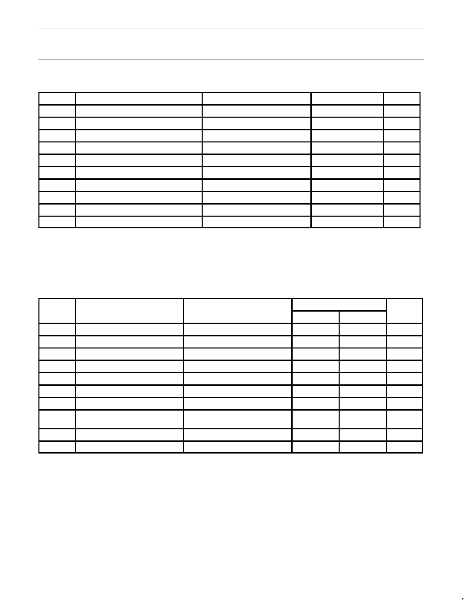
QUICK REFERENCE DATA
SYMBOL
PARAMETER
CONDITIONS
T
amb
= 25
∞
C; GND = 0V
TYPICAL
UNIT
t
PLH
Propagation delay
Sn to Dn
V
DD1
= 3.3V; V
DD2
= 2.5V;
V
REF
= 1.5V; unloaded
1.5
ns
C
OFF
Channel capacitance (OFF-state)
V
S
= 1.5V
7.5
pF
ORDERING INFORMATION
PACKAGES
TEMPERATURE RANGE
OUTSIDE NORTH AMERICA
NORTH AMERICA
DWG NUMBER
24-Pin Plastic TSSOP Type II
0
∞
C to +85
∞
C
GTL2010 PW
GTL2010PW DH
SOT355≠1
PIN DESCRIPTION
PIN NUMBER
SYMBOL
NAME AND FUNCTION
1
GND
Ground (0V)
2
S
REF
Source of reference
transistor
3 ≠ 12
S
n
Port S
1
to Port S
10
13 ≠ 22
D
n
Port D
1
to Port D
10
23
D
REF
Drain of reference
transistor
24
G
REF
Gate of reference
transistor
FUNCTION TABLE
S
N
D
N
L
L
H
H
H = High voltage level
L
= Low voltage level
Z = High impedance "off " state
CLAMP SCHEMATIC
S
REF
S
1
S
10
D
REF
D
1
D
10
G
REF
SA00526
Philips Semiconductors
Product specification
GTL2010
10-bit GTL Processor Voltage Clamp
1999 Apr 05
3
ABSOLUTE MAXIMUM RATINGS
1, 2, 3
SYMBOL
PARAMETER
CONDITIONS
RATING
UNIT
V
S_REF
DC source reference voltage
≠0.5 to +7.0
V
V
D_REF
DC drain reference voltage
≠0.5 to +7.0
V
V
G_REF
DC gate reference voltage
≠0.5 to +7.0
V
V
Sn
DC voltage Port S
n
≠0.5 to +7.0
V
V
Dn
DC voltage Port D
n
≠0.5 to +7.0
V
I
REFK
DC reference diode current
V
I
< 0
≠50
mA
I
SK
DC diode current Port S
n
V
I
< 0
≠50
mA
I
DK
DC diode current Port D
n
V
I
< 0
≠50
mA
I
MAX
DC clamp current per channel
Channel in ON-state
±
35
mA
T
stg
Storage temperature range
≠65 to +150
∞
C
NOTE:
1. Stresses beyond those listed may cause permanent damage to the device. These are stress ratings only and functional operation of the
device at these or any other conditions beyond those indicated under "recommended operating conditions" is not implied. Exposure to
absolute-maximum-rated conditions for extended periods may affect device reliability.
2. The performance capability of a high-performance integrated circuit in conjunction with its thermal environment can create junction
temperatures which are detrimental to reliability. The maximum junction temperature of this integrated circuit should not exceed 150
∞
C.
3. The input and output negative voltage ratings may be exceeded if the input and output clamp current ratings are observed.
RECOMMENDED OPERATING CONDITIONS
SYMBOL
PARAMETER
CONDITIONS
LIMITS
UNIT
SYMBOL
PARAMETER
CONDITIONS
Min
Max
UNIT
V
S_REF
DC source reference voltage
1.0
4.4
V
V
D_REF
DC drain reference voltage
V
S_REF
+ 0.6
5
V
V
G_REF
DC gate reference voltage
V
S_REF
+ 0.6
5
V
V
Sn
DC voltage Port S
n
(OFF-state)
V
S_REF
5
V
V
Sn
DC voltage Port S
n
(ON-state)
0
0.2
V
V
Dn
DC voltage Port D
n
(OFF-state)
V
S_REF
5
V
V
Dn
DC voltage Port D
n
(ON-state)
0
0.4
V
I
S
Switch input leakage current
(OFF-state) for S
n
and D
n
I/O
V
S
, V
D
= 5V
15
µ
A
I
I
G
REF
input leakage current
V
G
= 5V
2.5
µ
A
T
amb
Operating ambient temperature range
In free air
0
+85
∞
C
Philips Semiconductors
Product specification
GTL2010
10-bit GTL Processor Voltage Clamp
1999 Apr 05
4
DC CHARACTERISTICS for V
DD1
= 3.0 to 3.6V; V
DD2
= 2.36 to 2.64V; V
REF
= 1.365 to 1.635V range
Over recommended operating conditions. Voltage are referenced to GND (ground = 0V). Refer to the Test Circuit diagram.
LIMITS
SYMBOL
PARAMETER
TEST CONDITIONS
T
amb
= 0
∞
C to +85
∞
C
UNIT
Min
Typ
1
Max
V
OL
LOW level output voltage
V
S
= 0.175V; I
CLAMP
= 15.2mA
260
350
mV
NOTE:
1. All typical values are measured at V
DD1
= 3.3V, V
DD2
= 2.5V, V
REF
= 1.5V and T
amb
= 25 C
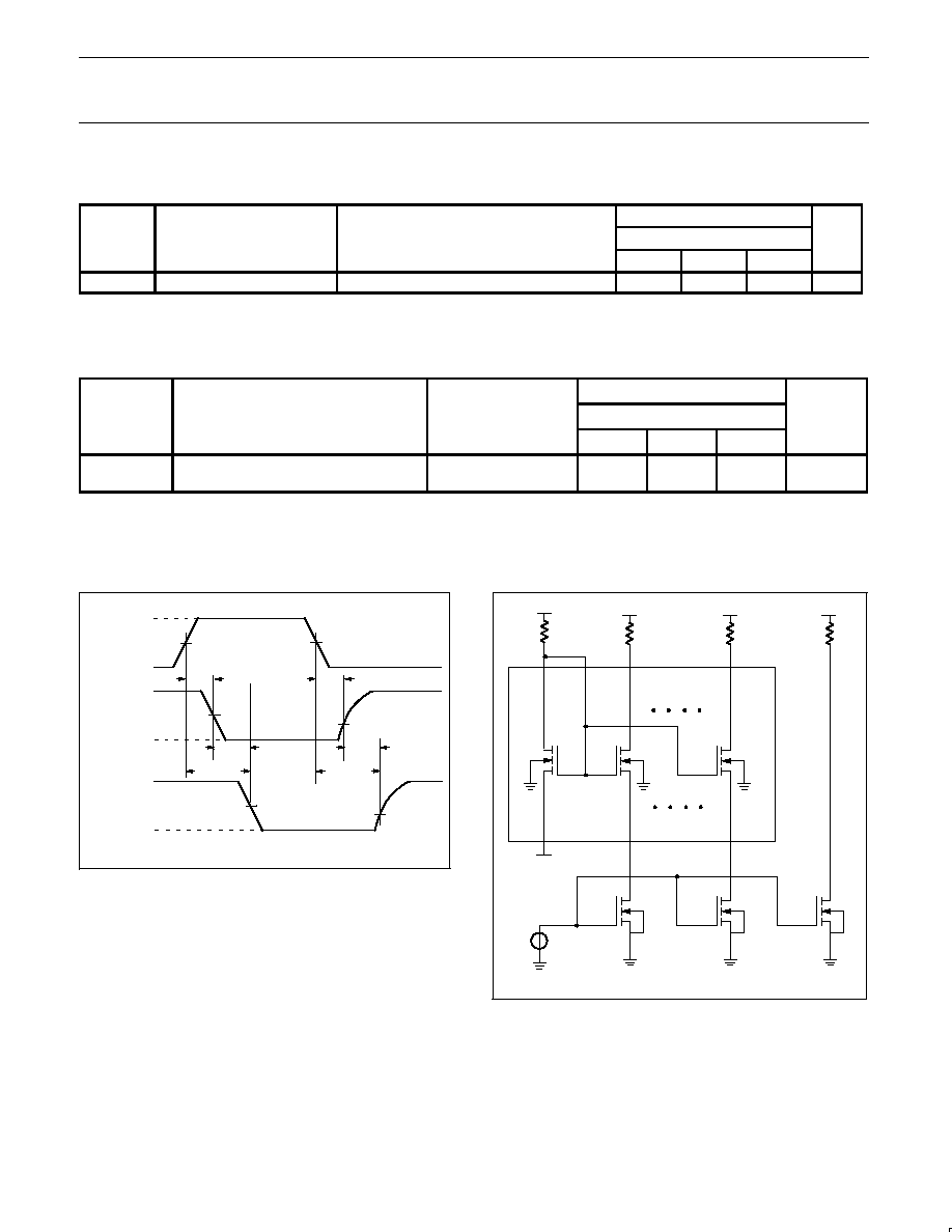
AC CHARACTERISTICS for V
DD1
= 3.0 to 3.6V; V
DD2
= 2.36 to 2.64V; V
REF
= 1.365 to 1.635V range
GND = 0V; t
r
= t
f
3.0ns Refer to the Test Circuit diagram.
LIMITS
SYMBOL
PARAMETER
WAVEFORM
T
amb
= 0 to +85
∞
C
UNIT
MIN
TYP
1
MAX
t
PLH
2
Propagation delay
Sn to Dn; Dn to Sn
0.5
1.5
5.5
ns
NOTE:
1. All typical values are measured at V
DD1
= 3.3V, V
DD2
= 2.5V, V
REF
= 1.5V and T
amb
= 25 C
2. Propagation delay guaranteed by characterization
3. C
ON,MAX
of 30pF and a C
OFF,MAX
of 15pF is guaranteed by design
AC WAVEFORMS
INPUT
t
PHL
t
PLH
V
M
V
M
V
M
V
M
OUTPUT
HIGH-to-LOW
LOW-to-HIGH
V
M
V
M
OUTPUT
HIGH-to-LOW
LOW-to-HIGH
V
I
GND
V
DD2
V
OL
V
DD2
V
OL
0
0
t
PHL1
t
PLH
1
t
PHL
t
PLH
SA00524
Waveform 1. The Input (S
n
) to Output (D
n
) Propagation Delays
TEST CIRCUIT
V
REF
S
1
S
10
D
REF
D
1
D
10
G
REF
PULSE
GENERATOR
DUT
S
REF
V
DD1
V
DD2
V
DD2
V
DD2
200K
150
150
150
SA00525
Waveform 2. Load circuit
Philips Semiconductors
Product specification
GTL2010
10-bit GTL Processor Voltage Clamp
1999 Apr 05
5
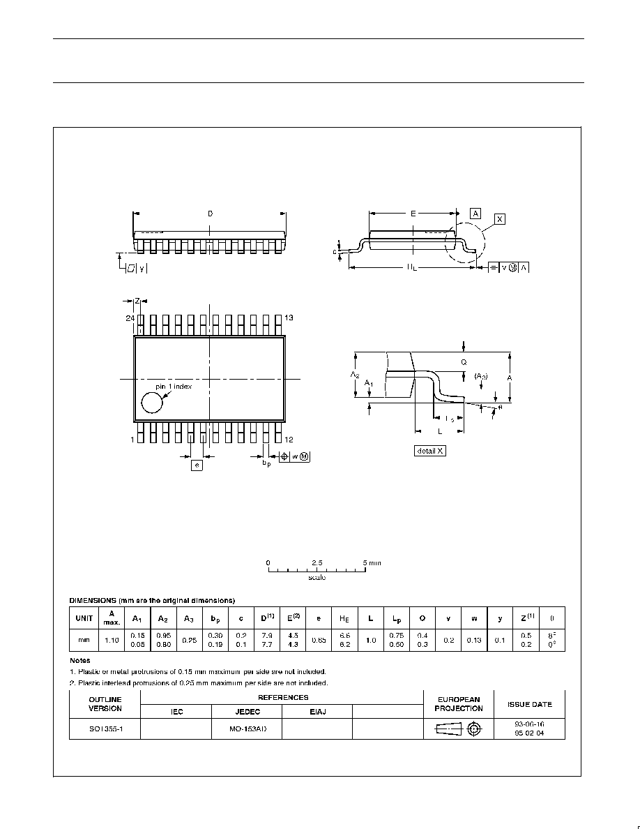
TSSOP24:
plastic thin shrink small outline package; 24 leads; body width 4.4 mm
SOT355-1
Philips Semiconductors
Product specification
GTL2010
10-bit GTL Processor Voltage Clamp
yyyy mmm dd
6
Definitions
Short-form specification -- The data in a short-form specification is extracted from a full data sheet with the same type number and title. For
detailed information see the relevant data sheet or data handbook.
Limiting values definition -- Limiting values given are in accordance with the Absolute Maximum Rating System (IEC 134). Stress above one
or more of the limiting values may cause permanent damage to the device. These are stress ratings only and operation of the device at these or
at any other conditions above those given in the Characteristics sections of the specification is not implied. Exposure to limiting values for extended
periods may affect device reliability.
Application information -- Applications that are described herein for any of these products are for illustrative purposes only. Philips
Semiconductors make no representation or warranty that such applications will be suitable for the specified use without further testing or
modification.
Disclaimers
Life support -- These products are not designed for use in life support appliances, devices or systems where malfunction of these products can
reasonably be expected to result in personal injury. Philips Semiconductors customers using or selling these products for use in such applications
do so at their own risk and agree to fully indemnify Philips Semiconductors for any damages resulting from such application.
Right to make changes -- Philips Semiconductors reserves the right to make changes, without notice, in the products, including circuits, standard
cells, and/or software, described or contained herein in order to improve design and/or performance. Philips Semiconductors assumes no
responsibility or liability for the use of any of these products, conveys no license or title under any patent, copyright, or mask work right to these
products, and makes no representations or warranties that these products are free from patent, copyright, or mask work right infringement, unless
otherwise specified.
Philips Semiconductors
811 East Arques Avenue
P.O. Box 3409
Sunnyvale, California 94088≠3409
Telephone 800-234-7381
©
Copyright Philips Electronics North America Corporation 1998
All rights reserved. Printed in U.S.A.
print code
Date of release: 10-98
Document order number:
9397-750-05519
Philips
Semiconductors
Data sheet
status
Objective
specification
Preliminary
specification
Product
specification
Product
status
Development
Qualification
Production
Definition
[1]
This data sheet contains the design target or goal specifications for product development.
Specification may change in any manner without notice.
This data sheet contains preliminary data, and supplementary data will be published at a later date.
Philips Semiconductors reserves the right to make chages at any time without notice in order to
improve design and supply the best possible product.
This data sheet contains final specifications. Philips Semiconductors reserves the right to make
changes at any time without notice in order to improve design and supply the best possible product.
Data sheet status
[1]
Please consult the most recently issued datasheet before initiating or completing a design.