GTLPH16612_1, 18-bit GTLP to LVTTL/TTL bidirectional universal translator (3-State)

Philips
Semiconductors
GTLPH16612
18-bit GTLP to LVTTL/TTL bidirectional
universal translator (3-State)
2001 Sep 28
INTEGRATED CIRCUITS
Product data
File under Integrated Ciruits ICL03
Philips Semiconductors
Product data
GTLPH16612
18-bit GTLP to LVTTL/TTL bidirectional
universal translator (3-State)
2
2001 Sep 28
8532285 27174
FEATURES
·
18-bit bidirectional bus interface
·
Translates between GTLP logic levels (B ports) and LVTTL/TTL
logic levels (A ports)
·
Edge rate control circuitry on the Bn outputs rising/falling edges to
minimize system noise in a multipoint backplane environment
·
5 V I/O tolerant on the LVTTL side
·
No bus current loading when LVTTL output is tied to 5 V bus
·
3-State buffers
·
Output capability: +64 mA/-32 mA on the LVTTL side; +40 mA on
the GTLP side
·
LVTTL input levels on control pins
·
Power-up reset
·
Power-up 3-State
·
Positive edge triggered clock inputs
·
Latch-up protection exceeds 500 mA per JESD78
·
ESD protection exceeds 2000 V HBM per JESD22-A114,
200 V MM per JESD22-A115 and 750 V (Bn I/O exceeds 1000 V)
CDM per JESD22-C101
DESCRIPTION
The GTLPH16612 is a high-performance BiCMOS product designed
for V
CC
operation at 3.3V with I/O compatibility up to 5 V.
The GTLPH16612 is unique in that pin 50 is a no connect and this
device can be used as a replacement device in sockets where
pin 50 is 3.3/5 V V
CC
or 3.3 V BIAS V
CC
.
This device is an 18-bit universal transceiver featuring non-inverting
3-State bus compatible outputs in both send and receive directions.
Data flow in each direction is controlled by output enable (OEAB and
OEBA), latch enable (LEAB and LEBA), and clock (CPAB and
CPBA) inputs. For A-to-B data flow, the device operates in the
transparent mode when LEAB is High. When LEAB is Low, the A
data is latched if CPAB is held at a High or Low logic level. If LEAB
is Low, the A-bus data is stored in the latch/flip-flop on the
Low-to-High transition of CPAB. When OEAB is Low, the outputs are
active. When OEAB is High, the outputs are in the high-impedance
state. The clocks can be controlled with the clock-enable inputs
(CEBA/CEAB).
Data flow for B-to-A is similar to that of A-to-B but uses OEBA,
LEBA and CPBA.
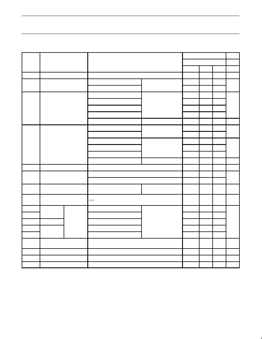
QUICK REFERENCE DATA
SYMBOL
PARAMETER
CONDITIONS
TYPICAL
UNIT
SYMBOL
PARAMETER
T
amb
= 25
°
C
3.3 V
UNIT
t
PLH
t
PHL
Propagation delay
An to Bn or Bn to An
C
L
= 50 pF
1.9
ns
C
IN
Input capacitance (Control pins)
V
I
= 0 V or V
CC
4
pF
C
I/O
An I/O pin capacitance
V
I/O
= 0 V or V
CC
9
pF
C
I/O
Bn I/O pin capacitance
V
I/O
= 0 V or 1.5 V
5.3
pF
I
CCZ
Total supply current
Outputs disabled
12
mA
ORDERING INFORMATION
PACKAGES
TEMPERATURE RANGE
ORDER CODE
DWG NUMBER
56-Pin Plastic SSOP
40 to +85
°
C
GTLPH16612DL
SOT371-1
56-Pin Plastic TSSOP
40 to +85
°
C
GTLPH16612DGG
SOT364-1
NOTE:
1. Standard packing quantities and other packaging data is available at www.philipslogic.com/support/packages.
Philips Semiconductors
Product data
GTLPH16612
18-bit GTLP to LVTTL/TTL bidirectional universal
translator (3-State)
2001 Sep 28
3
PIN CONFIGURATION
GND
GND
CEAB
GND
LEAB
OEAB
GND
VCC
NC
GND
GND
VCC
VREF
GND
CEBA
GND
LEBA
OEBA
1
2
3
4
5
6
7
8
9
10
11
12
13
14
15
16
17
18
19
20
21
22
23
24
25
26
27
28
29
30
31
32
33
34
35
36
37
38
39
40
41
42
43
44
45
46
47
48
49
50
51
52
53
54
55
56
A1
A2
A3
A4
A5
A6
A7
A8
A9
A10
A11
A12
A13
A14
A15
A16
A17
CPAB
B0
B2
B1
B3
B4
B5
B6
B7
B8
B9
B10
B11
B12
B13
B14
B15
B16
B17
CPBA
SW00486
A0
PIN DESCRIPTION
PIN NUMBER
SYMBOL
NAME AND FUNCTION
1, 27
OEAB/OEBA
A-to-B/ B-to-A Output
enable input (active Low)
29, 56
CEBA/CEAB
B-to-A/A-to-B clock
enable
2, 28
LEAB/LEBA
A-to-B/B-to-A Latch
enable input
55, 30
CPAB/CPBA
A-to-B/B-to-A Clock input
(active rising edge)
3, 5, 6, 8, 9, 10,
12, 13, 14, 15,
16, 17, 19, 20,
21, 23, 24, 26
A0-A17
Data inputs/outputs
(A side)
54, 52, 51, 49,
48, 47, 45, 44,
43, 42, 41, 40,
38, 37, 36, 34,
33, 31
B0-B17
Data inputs/outputs
(B side)
4, 11, 18, 25, 32,
39, 46, 53
GND
Ground (0V)
7, 22
V
CC
Positive supply voltage
35
V
REF
GTLP reference voltage
50
NC
No connect
Philips Semiconductors
Product data
GTLPH16612
18-bit GTLP to LVTTL/TTL bidirectional universal
translator (3-State)
2001 Sep 28
4
FUNCTION TABLE
INPUTS
OUTPUT
CEAB
OEAB
LEAB
CPAB
A
B
MODE
X
H
X
X
X
Z
Isolation
L
L
L
L
L
Clocked storage of A data
L
L
L
H
H
Clocked storage of A data
X
L
H
X
L
L
Transparent
X
L
H
X
H
H
Trans arent
L
L
L
H
X
B
O
Latched storage of A data
L
L
L
L
X
B
O
§
Latched storage of A data
H
L
L
X
X
B
O
Clock inhibit
X = Don't care
H = High voltage level
L = Low voltage level
= Low to High
Z = High impedance "off " state
= A-to-B data flow is shown: B-to-A flow is similar but uses OEBA, LEBA, CPBA, and CEBA. The condition when OEAB and OEBA are both
low at the same time is not recommended.
= Output level before the indicated steady-state input conditions were established.
§ = Output level before the indicated steady-state input conditions were established, provided that CPAB was Low before LEAB went Low.
LOGIC SYMBOL (Positive Logic)
CE
1D
1D
CE
OEAB
CEAB
CPAB
LEAB
CPBA
LEBA
1
56
55
2
28
30
54
B0
To 17 other channels
SW00894
CEBA
A0
OEBA
29
27
3
C1
CLK
C1
CLK
V
REF
35
Philips Semiconductors
Product data
GTLPH16612
18-bit GTLP to LVTTL/TTL bidirectional universal
translator (3-State)
2001 Sep 28
5
ABSOLUTE MAXIMUM RATINGS
1, 2
SYMBOL
PARAMETER
CONDITIONS
RATING
UNIT
V
CC
DC supply voltage
0.5 to +4.6
V
I
IK
DC input diode current
V
I
< 0 V
50
mA
V
DC input voltage
3
A port
0.5 to +7.0
V
V
I
DC input voltage
3
B port
0.5 to +4.6
V
I
OK
DC output diode current
V
O
< 0 V; A port
50
mA
V
O
DC output voltage
3
Output in Off or High state; A port
0.5 to +7.0
V
V
OUT
DC output voltage
3
Output in Off or High state; B port
0.5 to +4.6
V
I
O
Current into any output in the LOW state
A port
128
mA
I
OL
Current into any output in the LOW state
B port
80
mA
I
OH
Current into any output in the HIGH state
A port
64
mA
T
stg
Storage temperature range
65 to +150
°
C
NOTES:
1. Stresses beyond those listed may cause permanent damage to the device. These are stress ratings only and functional operation of the
device at these or any other conditions beyond those indicated under "recommended operating conditions" is not implied. Exposure to
absolute-maximum-rated conditions for extended periods may affect device reliability.
2. The performance capability of a high-performance integrated circuit in conjunction with its thermal environment can create junction
temperatures which are detrimental to reliability. The maximum junction temperature of this integrated circuit should not exceed 150
°
C.
3. The input and output negative voltage ratings may be exceeded if the input and output clamp current ratings are observed.
RECOMMENDED OPERATING CONDITIONS
1, 2
SYMBOL
PARAMETER
TEST CONDITIONS
3.3V RANGE LIMITS
UNIT
SYMBOL
PARAMETER
TEST CONDITIONS
MIN
TYP
MAX
UNIT
V
CC
DC supply voltage
3.0
3.3
3.6
V
V
Termination voltage
GTL
1.14
1.2
1.26
V
V
TT
Termination voltage
GTLP
1.35
1.5
1.65
V
V
GTL reference voltage
GTL
0.74
0.8
0.87
V
V
REF
GTL reference voltage
GTLP
0.9
1
1.10
V
V
Input voltage
B port
0
V
TT
Note 3
V
V
I
Input voltage
Except B port
0
V
CC
5.5
V
V
HIGH level input voltage
B port
V
REF
+50mV
--
--
V
V
IH
HIGH-level input voltage
Except B port
2.0
--
--
V
V
LOW level input voltage
B port
--
--
V
REF
50mV
V
V
IL
LOW-level input voltage
Except A port
--
--
0.8
V
I
OH
HIGH-level output current
A port
--
--
32
mA
B port, GTL
--
--
32
mA
I
OL
LOW-level output current
B port, GTLP
--
--
40
mA
A port
--
--
64
mA
t
/
v
Input transition rise or fall rate
Outputs enabled
--
--
10
ns/V
t
/
V
CC
Power-up rate
20
--
--
µ
s/V
T
amb
Operating free-air temperature range
40
--
+85
°
C
NOTES:
1. Normal connection sequence is GND first; V
CC
, I/O, control inputs, V
TT
and V
REF
(any order) last.
2. V
REF
can be adjusted to optimize noise margins, but normally is two-thirds V
TT
.
3. V
TT
and R
TT
can be adjusted to accommodate backplane impedances if the DC recommended I
OL
ratings are not exceeded and the
absolute max V
I
rating is not exceeded.
Philips Semiconductors
Product data
GTLPH16612
18-bit GTLP to LVTTL/TTL bidirectional universal
translator (3-State)
2001 Sep 28
6
DC ELECTRICAL CHARACTERISTICS (3.3 V
"
0.3 V RANGE)
LIMITS
SYMBOL
PARAMETER
TEST CONDITIONS
Temp = 40 to +85
°
C
UNIT
MIN
TYP
1
MAX
V
IK
Input clamp voltage
V
CC
= 3.0 V; I
IK
= 18 mA
--
0.85
1.2
V
V
O
High level output voltage
V
CC
= 3.0 to 3.6 V; I
OH
= 100
µ
A
A port
V
CC
0.2
V
CC
--
V
V
OH
High-level output voltage
V
CC
= 3.0 V; I
OH
= 32 mA
A port
2.0
2.3
--
V
V
CC
= 3.0 V; I
OL
= 100
µ
A
--
0.07
0.2
V
CC
= 3.0 V; I
OL
= 16 mA
A port
--
0.25
0.4
V
V
OL
Low-level output voltage
V
CC
= 3.0 V; I
OL
= 32 mA
A port
--
0.3
0.5
V
V
CC
= 3.0 V; I
OL
= 64 mA
--
0.4
0.55
V
CC
= 3.0 V; I
OL
= 40 mA
B port
--
0.4
0.5
V
V
CC
= 3.6 V; V
I
= V
CC
or GND
Control pins
--
0.1
±
1
µ
A
V
CC
= 0 or 3.6 V; V
I
= 5.5 V
Control pins
--
0.1
10
µ
A
I
Input leakage current
V
CC
= 3.6 V; V
I
= 5.5 V
4
--
0.1
20
I
I
Input leakage current
V
CC
= 3.6 V; V
I
= V
CC
I/O Data pins
4
A port
--
0.5
10
µ
A
V
CC
= 3.6 V; V
I
= 0 V
A ort
--
0.1
-5
V
CC
= 3.6 V; V
I
= V
TT
or GND
B port
--
--
±
5
µ
A
I
OFF
Output off current
V
CC
= 0 V; V
I
or V
O
= 0 to 4.5 V
--
0.1
±
100
µ
A
I
O
Bus Hold current A outputs
V
CC
= 3 V; V
I
= 0.8 V
75
130
--
µ
A
I
HOLD
Bus Hold current, A outputs
V
CC
= 3 V; V
I
= 2.0 V
75
140
--
µ
A
I
EX
Current into an output in the
High state when V
O
> V
CC
V
O
= 5.5 V; V
CC
= 3.0 V
A port
--
10
125
µ
A
I
PU/PD
Power up/down 3-State
output current
3
V
CC
1.2 V; V
O
= 0.5 V to V
CC
; V
I
= GND or V
CC
OE = Don't care
--
1.0
±
100
µ
A
I
CCH
A Port
Outputs high
--
5.0
9.0
I
CCL
A-Port
Outputs low
--
10.5
18.5
I
CCZ
5
V
CC
= 3.6 V
Disabled
V
I
= GND or V
CC
;
I
O
=
0
--
6.0
11.5
mA
I
CCH
B Port
Outputs high
I
O
0
--
9.7
17.5
I
CCL
B-Port
Outputs low
--
7.0
12.0
I
CC
Additional supply current per
input pin
2
V
CC
= 3 V to 3.6 V; One input at V
CC
0.6 V,
Other inputs at V
CC
or GND
--
0.04
0.2
mA
C
IN
Control pins capacitance
V
I
= 0 V or V
CC
--
4
--
pF
C
I/O
An I/O pin capacitance
V
I/O
= 0 V or V
CC
--
9.0
--
pF
C
I/O
Bn I/O pin capacitance
V
I/O
= 0 V or 1.5 V
--
5.3
7.3
6
pF
NOTES:
1. All typical values are at V
CC
= 3.3 V and T
amb
= 25
°
C.
2. This is the increase in supply current for each LVTTL input at the specified voltage level other than V
CC
or GND
3. This parameter is valid for any V
CC
between 0 V and 1.2 V with a transition time of up to 10 msec. From V
CC
= 1.2 V to V
CC
= 3.3 V
±
0.3 V
a transition time of 100
µ
sec is permitted. This parameter is valid for T
amb
= 25
°
C only.
4. Unused pins at V
CC
or GND.
5. I
CCZ
is measured with outputs pulled up to V
CC
or pulled down to ground.
6. The maximum Bn I/O pin capacitance is based on simulation data.
Philips Semiconductors
Product data
GTLPH16612
18-bit GTLP to LVTTL/TTL bidirectional universal
translator (3-State)
2001 Sep 28
7
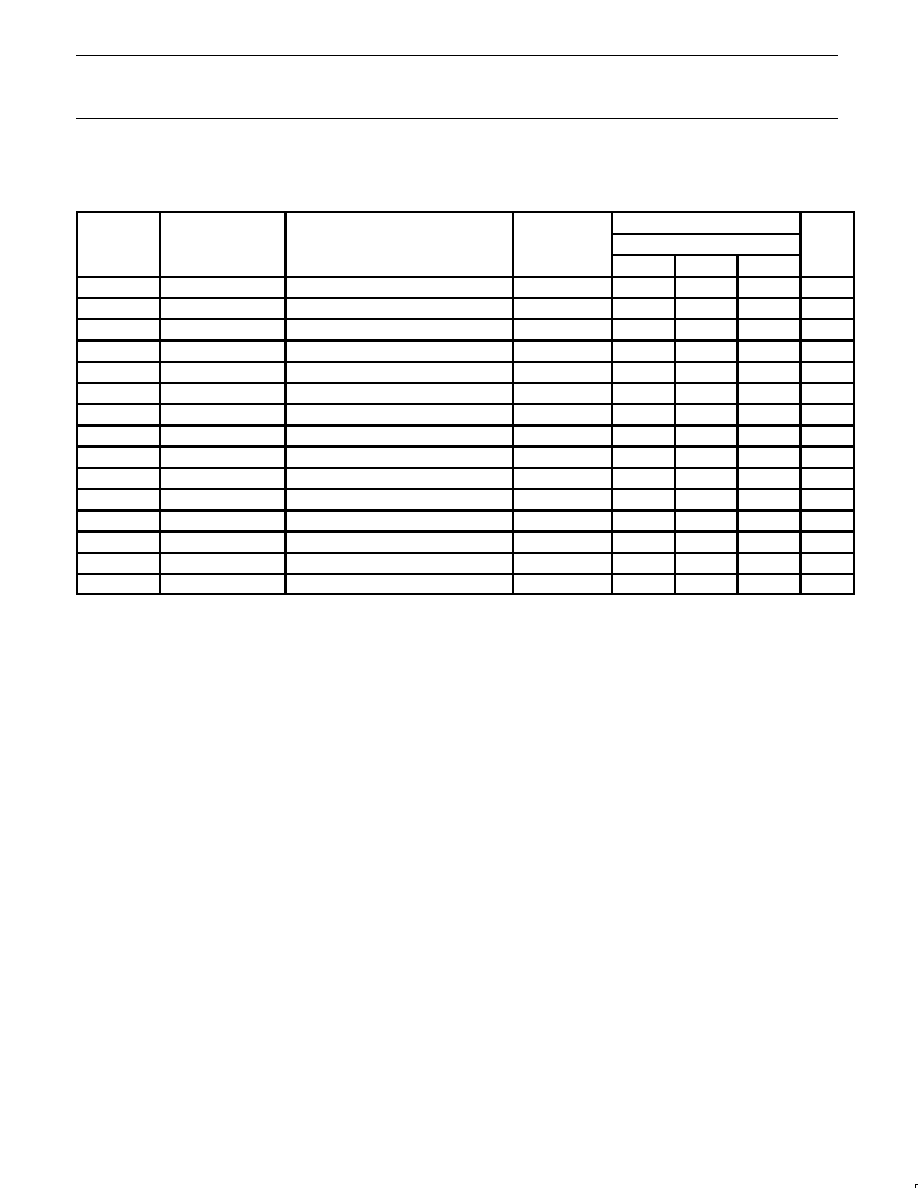
AC CHARACTERISTICS (A PORT)
GND = 0 V; t
r
= t
f
= 2.5 ns; C
L
= 50 pF; R
L
= 500
; T
amb
= 40 to +85
°
C.
GTLP
GTLPH16612 An Port
V
CC
= 3.3 V
±
0.3 V
UNIT
V
REF
= 1.0 V
UNIT
SYMBOL
PARAMETER
WAVEFORM
MIN
TYP
1
MAX
F
max
250
290
--
MHz
t
PLH
Bn to An
2
1.5
2.6
5.5
ns
t
PHL
Bn to An
2
2.6
4.3
6.5
ns
t
PLH
LEBA to An
3
1.6
3.0
4.9
ns
t
PHL
LEBA to An
3
2.0
3.0
4.5
ns
t
PLH
CPBA to An
1
1.1
2.7
4.9
ns
t
PHL
CPBA to An
1
1.8
3.0
4.6
ns
t
PZH
OEBA to An
5
1.5
4.3
6.2
ns
t
PHZ
OEBA to An
5
1.4
3.6
4.8
ns
t
PZL
OEBA to An
6
1.5
3.8
6.2
ns
t
PLZ
OEBA to An
6
1.0
2.6
5.5
ns
NOTE:
1. Typical values are at V
CC
= 3.3 V, T
amb
= +25
°
C.
AC CHARACTERISTICS (B PORT)
GND = 0 V; t
r
= t
f
= 2.5 ns; C
L
= 30 pF; R
L
= 25
; T
amb
= 40 to +85
°
C.
GTLP
GTLPH16612 Bn Port
V
CC
= 3.3 V
±
0.3 V
UNIT
V
REF
= 1.0 V
UNIT
SYMBOL
PARAMETER
WAVEFORM
MIN
TYP
1
MAX
F
max
250
270
--
MHz
t
PLH
An to Bn
2
1.8
4.8
9.0
ns
t
PHL
An to Bn
2
1.0
3.9
8.2
ns
t
PLH
LEAB to Bn
3
1.9
4.6
8.4
ns
t
PHL
LEAB to Bn
3
1.9
4.5
8.0
ns
t
PLH
CPAB to Bn
1
2.7
5.1
8.7
ns
t
PHL
CPAB to Bn
1
2.2
4.9
8.6
ns
t
PLH
OEAB to Bn
7
1.4
4.2
8.3
ns
t
PHL
OEAB to Bn
7
1.5
5.0
9.5
ns
t
rise
Transition time B outputs 20% to 80%
--
3.1
--
ns
t
fall
Transition time B outputs 20% to 80%
--
4.6
--
ns
NOTE:
1. Typical values are at V
CC
= 3.3 V, T
amb
= +25
°
C.
Philips Semiconductors
Product data
GTLPH16612
18-bit GTLP to LVTTL/TTL bidirectional universal
translator (3-State)
2001 Sep 28
8
AC SETUP REQUIREMENTS (3.3 V
±
0.3 V RANGE)
A Port:
GND = 0 V; Input t
r
= t
f
= 2.5 ns; C
L
= 50 pF; R
L
= 500
; T
amb
= 40 to +85
°
C; V
REF
= 0.8 V or 1.0 V.
B Port:
GND = 0 V; Input t
r
= t
f
= 2.5 ns; C
L
= 30 pF; R
L
= 25
; V
REF
= 0.8 V or 1.0 V.
LIMITS
SYMBOL
DESCRIPTION
PARAMETER
WAVEFORM
V
CC
= 3.3 V
±
0.3 V
UNIT
MIN
TYP
MAX
t
w
(H)
Pulse duration
LEAB or LEBA
3
1.0
--
--
ns
t
w
(H or L)
Pulse duration
CPAB or CPBA
4
2.5
--
--
ns
t
s
(H or L)
Setup time
An before CPAB rising edge
4
2.0
--
--
ns
t
s
(H)
Setup time
Bn before CPBA rising edge
4
2.5
--
--
ns
t
s
(L)
Setup time
Bn before CPBA rising edge
4
3.1
--
--
ns
t
s
(H or L)
Setup time
An before LEAB falling edge
4
0.5
--
--
ns
t
s
(H or L)
Setup time
Bn before LEBA falling edge
4
2.5
--
--
ns
t
s
(L)
Setup time
CEAB before CPAB rising edge
4
0
--
--
ns
t
s
(L)
Setup time
CEBA before CPBA rising edge
4
0
--
--
ns
t
h
(H or L)
Hold time
An after CPAB rising edge
4
0
--
--
ns
t
h
(H or L)
Hold time
Bn after CPBA rising edge
4
0
--
--
ns
t
h
(H or L)
Hold time
An after LEAB falling edge
4
0.5
--
--
ns
t
h
(H or L)
Hold time
Bn after LEBA falling edge
4
0
--
--
ns
t
h
(H)
Hold time
CEAB after CPAB rising edge
4
1.1
--
--
ns
t
h
(H)
Hold time
CEBA after CPBA rising edge
4
1.1
--
--
ns
Philips Semiconductors
Product data
GTLPH16612
18-bit GTLP to LVTTL/TTL bidirectional universal
translator (3-State)
2001 Sep 28
9
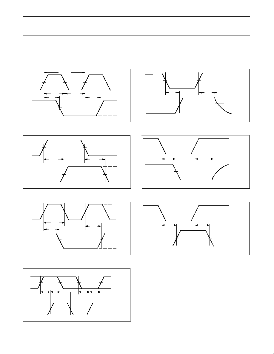
AC WAVEFORMS
V
M
= 1.5 V at V
CC
w
3.0 V.
V
M
= 1.5 V for A ports and control pins; V
M
= 1.0 V for B ports in GTLP mode.
V
X
= V
OL
+ 0.3 V at V
CC
w
3.0 V.
V
Y
= V
OH
0.3 V at V
CC
w
3.0 V.
t
PHL
t
PLH
VM
V
OH
t
W
(L)
1/f
MAX
CPBA or
CPAB
An or Bn
t
W
(H)
SW00181
VM
VM
VM
V
OL
3.0 V or V
CC
,
whichever is
less
0 V
Waveform 1.
Propagation delay, clock input to output, clock
pulse width, and maximum clock frequency
V
OL
t
PLH
V
OH
0 V
An or Bn
An or Bn
V
M
V
M
t
PHL
V
M
V
M
SW00176
3.0 V or V
CC
,
whichever is
less
Waveform 2.
Propagation delay, transparent mode
t
PLH
t
PHL
t
W
(H)
V
M
V
M
V
M
V
M
V
M
LEAB or
LEBA
An or Bn
0 V
V
OH
V
OL
SW00177
3.0 V or V
CC
,
whichever is
less
Waveform 3.
Propagation delay, enable to output,
and enable pulse width
ÉÉÉ
ÉÉÉ
ÉÉÉ
ÉÉÉÉ
ÉÉÉÉ
ÉÉÉÉ
ÉÉÉ
ÉÉÉ
ÉÉÉ
V
M
V
M
V
M
V
M
V
M
V
M
0V
An or Bn
CEAB or CEBA
CPAB or CPBA,
LEAB or LEBA
t
S
(H)
t
h
(H)
t
S
(L)
t
h
(L)
0V
3.0 V or V
CC
,
whichever is
less
3.0 V or V
CC
,
whichever is
less
SW00222
Waveform 4.
Data setup and hold times
OEBA
An or Bn
t
PZH
t
PHZ
V
OH
V
Y
V
M
V
M
V
M
3.0 V or V
CC
,
whichever is
less
SW00223
Waveform 5.
3-State output enable time to high level
and output disable time from high level
V
OL
OEBA
t
PZL
t
PLZ
An or Bn
V
X
V
M
V
M
V
M
3.0 V or V
CC
,
whichever is
less
SW00224
Waveform 6.
3-State output enable time to low level
and output disable time from low level
V
OL
OEAB
t
PLH
Bn
V
M
V
M
3.0 V or V
CC
,
whichever is
less
SW00495
t
PHL
V
M
V
M
Waveform 7.
Output enable time on open collector output
with pull-up
Philips Semiconductors
Product data
GTLPH16612
18-bit GTLP to LVTTL/TTL bidirectional universal
translator (3-State)
2001 Sep 28
10
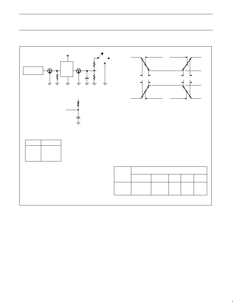
TEST CIRCUIT
PULSE
GENERATOR
VIN
VOUT
CL
VCC
Test Circuit for A Outputs
VM
VM
tW
NEGATIVE
PULSE
10%
10%
90%
90%
0 V
VM
VM
tW
POSITIVE
PULSE
90%
90%
10%
10%
0 V
tTHL (tF)
tTLH (tR)
tTHL (tF)
tTLH (tR)
DEFINITIONS
R
L
=
Load resistor; see AC CHARACTERISTICS for value.
C
L
=
Load capacitance includes jig and probe capacitance:
See AC CHARACTERISTICS for value.
R
T
=
Termination resistance should be equal to Z
OUT
of
pulse generators.
INPUT PULSE REQUIREMENTS
FAMILY
GTLP
SWITCH POSITION
TEST
SWITCH
t
PLZ/
t
PZL
6 V
t
PLH/
t
PHL
Open
t
PHZ
/t
PZH
GND
6.0 V or V
CC
x 2
R
T
R
L
=
500
Open
GND
D.U.T.
Amplitude
Rep. Rate
t
W
t
R
t
F
3.0 V or V
CC
whichever
is less
v
10 MHz
500 ns
v
2.5 ns
v
2.5 ns
VIN
VIN
SW00255
Load Circuit for B Outputs
1.2 V
TEST POINT
FROM OUTPUT
UNDER TEST
C
L
= 30 pF
(INCLUDES PROBE AND JIG CAPACITANCE)
25
R
L
=
500
Input Waveforms
Philips Semiconductors
Product data
GTLPH16612
18-bit GTLP to LVTTL/TTL bidirectional universal
translator (3-State)
2001 Sep 28
11
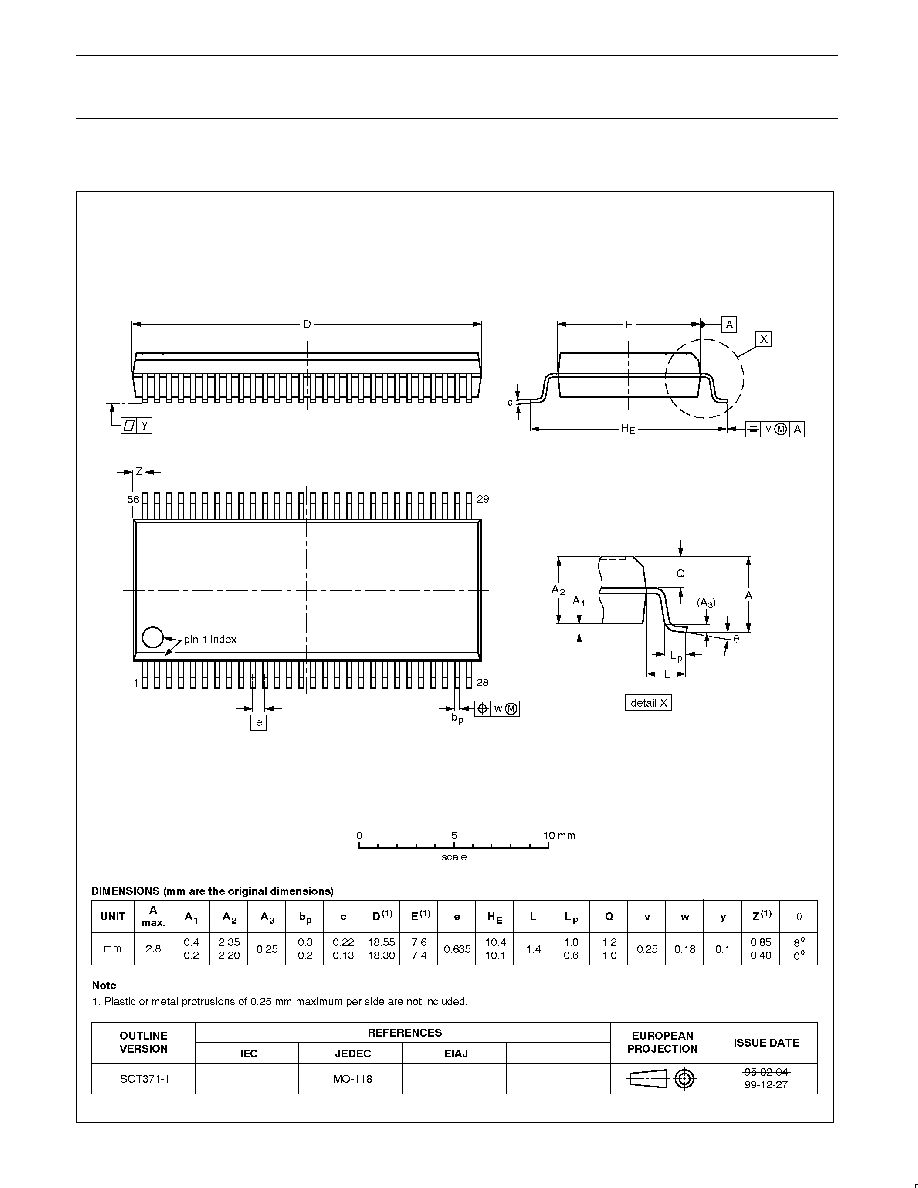
SSOP56:
plastic shrink small outline package; 56 leads; body width 7.5 mm
SOT371-1

Philips Semiconductors
Product data
GTLPH16612
18-bit GTLP to LVTTL/TTL bidirectional universal
translator (3-State)
2001 Sep 28
12
TSSOP56:
plastic thin shrink small outline package; 56 leads; body width 6.1 mm
SOT364-1

Philips Semiconductors
Product data
GTLPH16612
18-bit GTLP to LVTTL/TTL bidirectional universal
translator (3-State)
2001 Sep 28
13
NOTES
Philips Semiconductors
Product data
GTLPH16612
18-bit GTLP to LVTTL/TTL bidirectional universal
translator (3-State)
2001 Sep 28
14
Definitions
Short-form specification -- The data in a short-form specification is extracted from a full data sheet with the same type number and title. For
detailed information see the relevant data sheet or data handbook.
Limiting values definition -- Limiting values given are in accordance with the Absolute Maximum Rating System (IEC 60134). Stress above one
or more of the limiting values may cause permanent damage to the device. These are stress ratings only and operation of the device at these or
at any other conditions above those given in the Characteristics sections of the specification is not implied. Exposure to limiting values for extended
periods may affect device reliability.
Application information -- Applications that are described herein for any of these products are for illustrative purposes only. Philips
Semiconductors make no representation or warranty that such applications will be suitable for the specified use without further testing or
modification.
Disclaimers
Life support -- These products are not designed for use in life support appliances, devices or systems where malfunction of these products can
reasonably be expected to result in personal injury. Philips Semiconductors customers using or selling these products for use in such applications
do so at their own risk and agree to fully indemnify Philips Semiconductors for any damages resulting from such application.
Right to make changes -- Philips Semiconductors reserves the right to make changes, without notice, in the products, including circuits, standard
cells, and/or software, described or contained herein in order to improve design and/or performance. Philips Semiconductors assumes no
responsibility or liability for the use of any of these products, conveys no license or title under any patent, copyright, or mask work right to these
products, and makes no representations or warranties that these products are free from patent, copyright, or mask work right infringement, unless
otherwise specified.
Contact information
For additional information please visit
http://www.semiconductors.philips.com.
Fax: +31 40 27 24825
For sales offices addresses send e-mail to:
sales.addresses@www.semiconductors.philips.com.
©
Koninklijke Philips Electronics N.V. 2001
All rights reserved. Printed in U.S.A.
Date of release: 09-01
Document order number:
9397 750 08911
Philips
Semiconductors
Data sheet status
[1]
Objective data
Preliminary data
Product data
Product
status
[2]
Development
Qualification
Production
Definitions
This data sheet contains data from the objective specification for product development.
Philips Semiconductors reserves the right to change the specification in any manner without notice.
This data sheet contains data from the preliminary specification. Supplementary data will be
published at a later date. Philips Semiconductors reserves the right to change the specification
without notice, in order to improve the design and supply the best possible product.
This data sheet contains data from the product specification. Philips Semiconductors reserves the
right to make changes at any time in order to improve the design, manufacturing and supply.
Changes will be communicated according to the Customer Product/Process Change Notification
(CPCN) procedure SNW-SQ-650A.
Data sheet status
[1] Please consult the most recently issued data sheet before initiating or completing a design.
[2] The product status of the device(s) described in this data sheet may have changed since this data sheet was published. The latest information is available on the Internet at URL
http://www.semiconductors.philips.com.
Document Outline
- FEATURES
- DESCRIPTION
- QUICK REFERENCE DATA
- ORDERING INFORMATION
- PIN CONFIGURATION
- PIN DESCRIPTION
- FUNCTION TABLE
- LOGIC SYMBOL
- ABSOLUTE MAXIMUM RATINGS 1, 2
- RECOMMENDED OPERATING CONDITIONS 1, 2
- DC ELECTRICAL CHARACTERISTICS (3.3 V
- AC CHARACTERISTICS (A PORT)
- AC CHARACTERISTICS (B PORT)
- AC SETUP REQUIREMENTS (3.3 V ±0.3 V RANGE)
- AC WAVEFORMS
- TEST CIRCUIT
- PACKAGE