DATA SHEET
Product specification
File under Integrated Circuits, IC04
January 1995
INTEGRATED CIRCUITS
HEF40098B
buffers
3-state hex inverting buffer
For a complete data sheet, please also download:
∑
The IC04 LOCMOS HE4000B Logic
Family Specifications HEF, HEC
∑
The IC04 LOCMOS HE4000B Logic
Package Outlines/Information HEF, HEC
January 1995
2
Philips Semiconductors
Product specification
3-state hex inverting buffer
HEF40098B
buffers
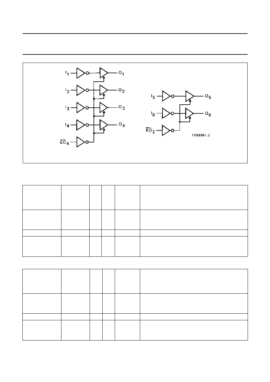
DESCRIPTION
The HEF40098B is a hex inverting buffer with 3-state
outputs. The 3-state outputs are controlled by two enable
inputs (EO
4
and EO
2
). A HIGH on EO
4
causes four of the
six buffer elements to assume a high impedance or
OFF-state regardless of the other input conditions and a
HIGH on EO
2
causes the outputs of the remaining two
buffer elements to assume a high impedance or OFF-state
regardless of the other input conditions.
Fig.1 Functional diagram.
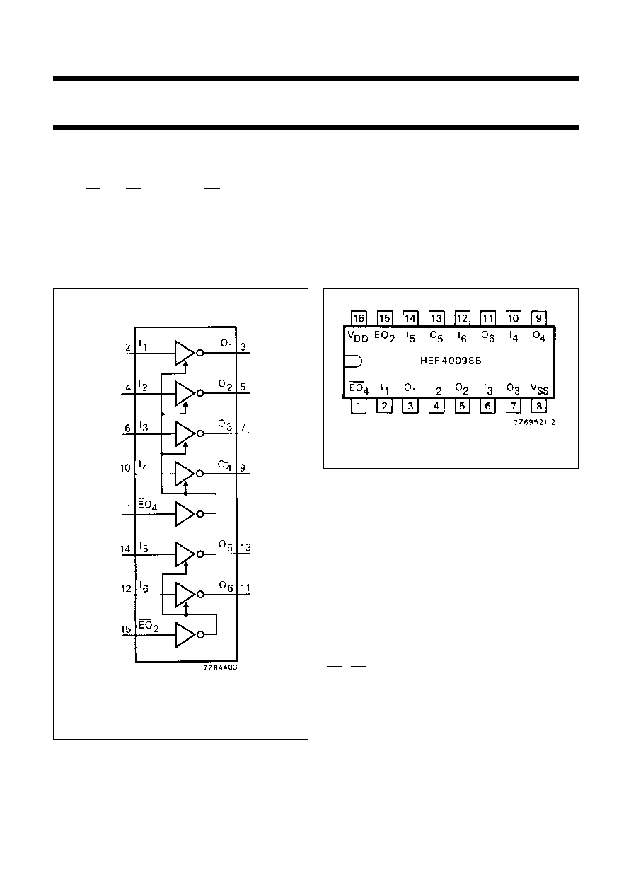
PINNING
FAMILY DATA, I
DD
LIMITS category BUFFERS
See Family Specifications
HEF40098BP(N):
16-lead DIL; plastic
(SOT38-1)
HEF40098BD(F):
16-lead DIL; ceramic (cerdip)
(SOT74)
HEF40098BT(D):
16-lead SO; plastic
(SOT109-1)
( ): Package Designator North America
I
1
to I
6
buffer inputs
EO
4
, EO
2
enable inputs (active LOW)
O
1
to O
6
buffer outputs (active LOW)
Fig.2 Pinning diagram.
January 1995
4
Philips Semiconductors
Product specification
3-state hex inverting buffer
HEF40098B
buffers
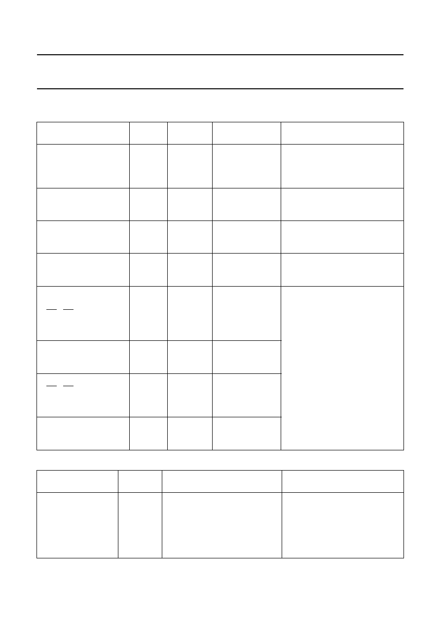
AC CHARACTERISTICS
V
SS
= 0 V; T
amb
= 25
∞
C; C
L
= 50 pF; input transition times
20 ns
V
DD
V
SYMBOL
TYP.
MAX.
TYPICAL EXTRAPOLATION
FORMULA
Propagation delays
I
n
O
n
5
80
160
ns
70 ns
+
(0,20 ns/pF) C
L
HIGH to LOW
10
t
PHL
35
70
ns
31 ns
+
(0,08 ns/pF) C
L
15
25
50
ns
22 ns
+
(0,06 ns/pF) C
L
5
65
130
ns
50 ns
+
(0,30 ns/pF) C
L
LOW to HIGH
10
t
PLH
30
60
ns
24 ns
+
(0,13 ns/pF) C
L
15
25
50
ns
23 ns
+
(0,05 ns/pF) C
L
Output transition times
5
30
60
ns
15 ns
+
(0,30 ns/pF) C
L
HIGH to LOW
10
t
THL
15
30
ns
10 ns
+
(0,11 ns/pF) C
L
15
10
20
ns
7 ns
+
(0,07 ns/pF) C
L
5
35
70
ns
10 ns
+
(0,50 ns/pF) C
L
LOW to HIGH
10
t
TLH
20
40
ns
8 ns
+
(0,24 ns/pF) C
L
15
15
30
ns
6 ns
+
(0,18 ns/pF) C
L
3-state propagation delays
Output disable times
EO
2
, EO
4
O
n
5
45
85
ns
HIGH
10
t
PHZ
35
65
ns
15
30
60
ns
5
65
135
ns
LOW
10
t
PLZ
40
80
ns
15
35
70
ns
Output enable times
EO
2
, EO
4
O
n
5
70
140
ns
HIGH
10
t
PZH
35
75
ns
15
30
65
ns
5
90
185
ns
LOW
10
t
PZL
40
85
ns
15
35
70
ns
V
DD
V
TYPICAL FORMULA FOR P (
µ
W)
Dynamic power
5
5 000 f
i
+
(f
o
C
L
)
◊
V
DD
2
where
dissipation per
10
22 800 f
i
+
(f
o
C
L
)
◊
V
DD
2
f
i
= input freq. (MHz)
package (P)
15
81 000 f
i
+
(f
o
C
L
)
◊
V
DD
2
f
o
= output freq. (MHz)
C
L
= load cap. (pF)
(f
o
C
L
) = sum of outputs
V
DD
= supply voltage (V)