DATA SHEET
Product specification
File under Integrated Circuits, IC04
January 1995
INTEGRATED CIRCUITS
HEF40175B
MSI
Quadruple D-type flip-flop
For a complete data sheet, please also download:
∑
The IC04 LOCMOS HE4000B Logic
Family Specifications HEF, HEC
∑
The IC04 LOCMOS HE4000B Logic
Package Outlines/Information HEF, HEC
January 1995
2
Philips Semiconductors
Product specification
Quadruple D-type flip-flop
HEF40175B
MSI
DESCRIPTION
The HEF40175B is a quadruple edge-triggered D-type
flip-flop with four data inputs (D
0
to D
3
), a clock input (CP),
an overriding asynchronous master reset input (MR), four
buffered outputs (O
0
to O
3
), and four complementary
buffered outputs (O
0
to O
3
). Information on D
0
to D
3
is
transferred to O
0
to O
3
on the LOW to HIGH transition of
CP if MR is HIGH. When LOW, MR resets all flip-flops
(O
0
to O
3
= LOW, O
0
to O
3
= HIGH), independent of CP
and D
0
to D
3
.
Fig.1 Functional diagram.
FAMILY DATA, I
DD
LIMITS category MSI
See Family Specifications
HEF40175BP(N): 16-lead DIL; plastic
(SOT38-1)
HEF40175BD(F):
16-lead DIL; ceramic (cerdip)
(SOT74)
HEF40175BT(D):
16-lead SO; plastic
(SOT109-1)
( ): Package Designator North America
Fig.2 Pinning diagram.
PINNING
FUNCTION TABLE
Notes
1. H = HIGH state (the more positive voltage)
L = LOW state (the less positive voltage)
X = state is immaterial
= positive-going transition
= negative-going transition
D
0
to D
3
data inputs
CP
clock input (LOW to HIGH; edge-triggered)
MR
master reset input (active LOW)
O
0
to O
3
buffered outputs
O
0
to O
3
complementary buffered outputs
INPUTS
OUTPUTS
CP
D
MR
O
O
H
H
H
L
L
H
L
H
X
H
no change
no change
X
X
L
L
H
January 1995
3
Philips Semiconductors
Product specification
Quadruple D-type flip-flop
HEF40175B
MSI
This text is here in white to force landscape pages to be rotated correctly when browsing through the pdf in the Acrobat reader.This text is here in
_
white to force landscape pages to be rotated correctly when browsing through the pdf in the Acrobat reader.This text is here inThis text is here in
white to force landscape pages to be rotated correctly when browsing through the pdf in the Acrobat reader. white to force landscape pages to be ...
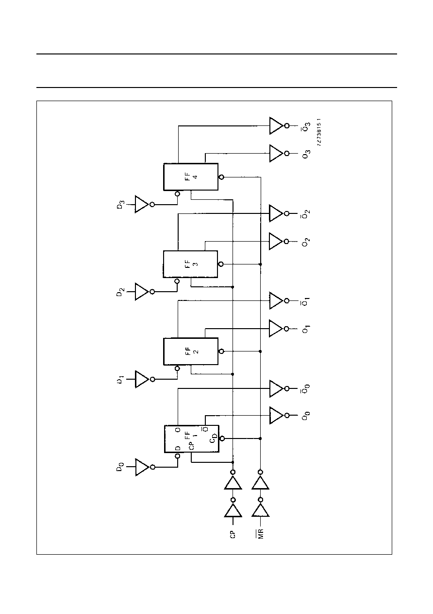
Fig.3 Logic diagram.
January 1995
5
Philips Semiconductors
Product specification
Quadruple D-type flip-flop
HEF40175B
MSI
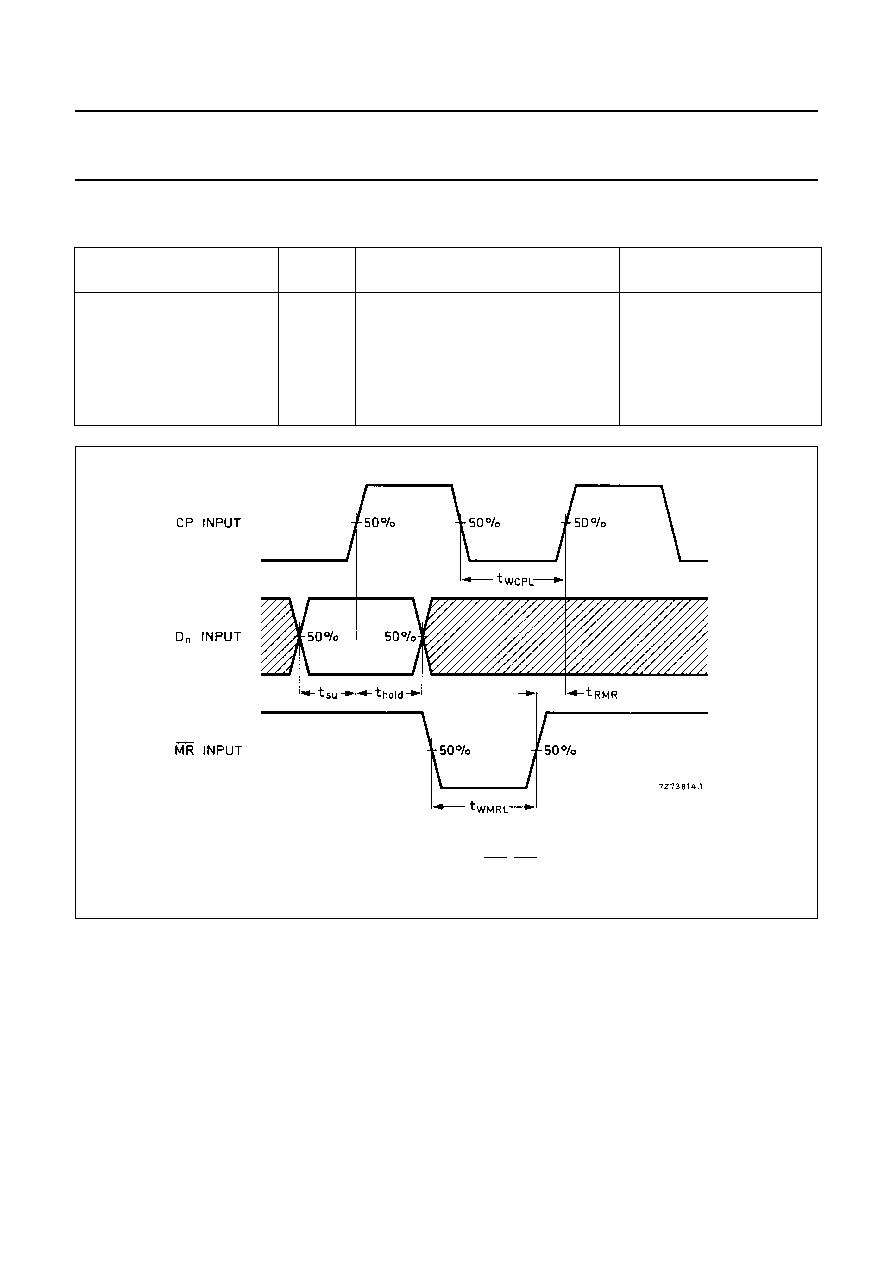
AC CHARACTERISTICS
V
SS
= 0 V; T
amb
= 25
∞
C; input transition times
20 ns
APPLICATION INFORMATION
Some examples of applications for the HEF40175B are:
∑
Shift registers
∑
Buffer/storage register
∑
Pattern generator
V
DD
V
TYPICAL FORMULA FOR P (
µ
W)
Dynamic power
5
2000 f
i
+
(f
o
C
L
)
◊
V
DD
2
where
dissipation per
10
8400 f
i
+
(f
o
C
L
)
◊
V
DD
2
f
i
= input freq. (MHz)
package (P)
15
22 500 f
i
+
(f
o
C
L
)
◊
V
DD
2
f
o
= output freq. (MHz)
C
L
= load capacitance (pF)
(f
o
C
L
) = sum of outputs
V
DD
= supply voltage (V)
Fig.4
Waveforms showing minimum pulse widths for CP and MR, MR to CP recovery time, and set-up time and
hold time for D
n
to CP. Set-up and hold times are shown as positive values but may be specified as
negative values.