
DATA SHEET
Product specification
File under Integrated Circuits, IC04
January 1995
INTEGRATED CIRCUITS
HEF40244B
buffers
Octal buffers with 3-state outputs
For a complete data sheet, please also download:
∑
The IC04 LOCMOS HE4000B Logic
Family Specifications HEF, HEC
∑
The IC04 LOCMOS HE4000B Logic
Package Outlines/Information HEF, HEC
January 1995
2
Philips Semiconductors
Product specification
Octal buffers with 3-state outputs
HEF40244B
buffers
DESCRIPTION
The HEF40244B is an octal non-inverting buffer with
3-state outputs. It features output stages with high current
output capability suitable for driving highly capacitive
loads.
The 3-state outputs are controlled by the output enable
inputs EO
A
and EO
B
. A HIGH on EO causes the outputs to
assume a high impedance OFF-state. The device also
features hysteresis on all inputs to improve noise
immunity.
Schmitt-trigger action in the inputs makes the circuit highly
tolerant to slower input rise and fall times.
The HEF40244B is pin and functionally compatible with
the TTL `244' device.
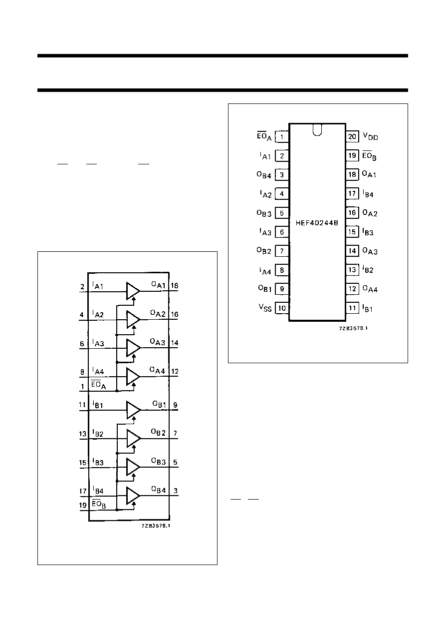
Fig.1 Functional diagram.
PINNING
FAMILY DATA, I
DD
LIMITS category buffers
See Family Specifications
HEF40244BP(N): 20-lead DIL; plastic (SOT146-1)
HEF40244BD(F):
20-lead DIL; ceramic (cerdip) (SOT152)
HEF40244BT(D):
20-lead SO; plastic (SOT163-1)
( ): Package Designator North America
I
A1
to I
A4
inputs
I
B1
to I
B4
inputs
O
A1
to O
A4
bus outputs
O
B1
to O
B4
bus outputs
EO
A
, EO
B
output enable inputs (active LOW)
Fig.2 Pinning diagram.
January 1995
3
Philips Semiconductors
Product specification
Octal buffers with 3-state outputs
HEF40244B
buffers
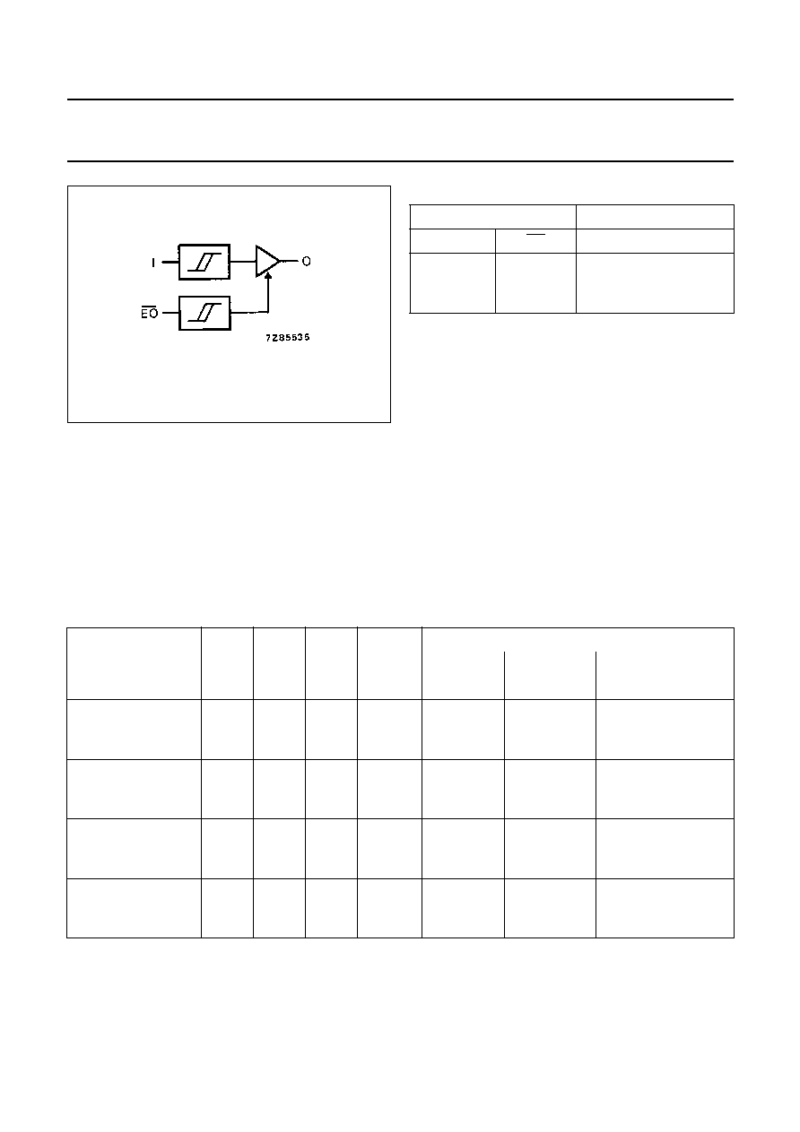
Fig.3 Logic diagram (one buffer).
TRUTH TABLE
Notes
1. H = HIGH state (the more positive voltage)
L = LOW state (the less positive voltage)
X = state is immaterial
Z = high impedance off state
INPUTS
OUTPUT
I
n
EO
O
n
H
L
H
L
L
L
X
H
Z
RATINGS
Limiting values in accordance with the Absolute Maximum System (IEC 134).
See Family Specifications, except for:
DC CHARACTERISTICS
V
SS
= 0 V
D.C. current into any input
±
I
I
max.
10 mA
D.C. source or sink current into any output
±
I
O
max.
25 mA
D.C. current into the supply terminals
±
I
max.
100 mA
V
DD
V
V
OH
V
V
OL
V
SYMBOL
T
amb
(
∞
C)
-
40
+
25
+
85
MIN.
TYP.
MIN.
TYP.
MIN.
TYP.
Output current
5
4,6
0,75
0,6
1,2
0,45
mA
HIGH
10
9,5
-
I
OH
1,85
1,5
3,0
1,1
mA
15
13,5
14,5
15
50
15,5
mA
Output current
5
3,6
9,3
10
24
10,7
mA
HIGH
10
8,4
-
I
OH
14,4
15
46
15,0
mA
15
13,2
19,5
20
62
19,8
mA
Output current
5
0,4
2,9
2,3
5,4
1,75
mA
LOW
10
0,5 I
OL
9,5
7,6
17
5,50
mA
15
1,5
30,0
25
45
19,0
mA
Hysteresis
5
220
mV
voltage
10
V
H
250
mV
(any input)
15
320
mV
January 1995
4
Philips Semiconductors
Product specification
Octal buffers with 3-state outputs
HEF40244B
buffers
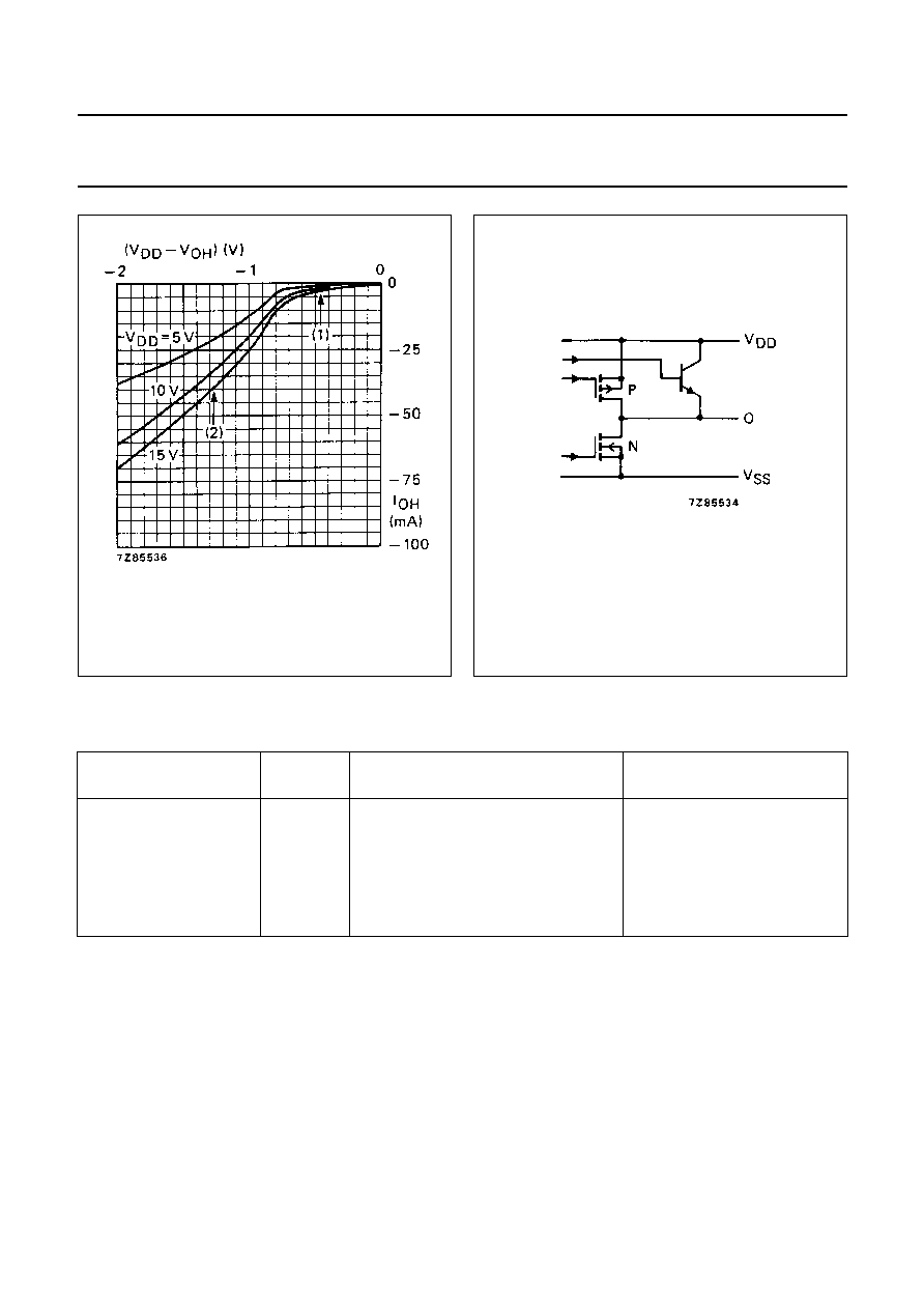
Fig.4 Typical output source current characteristic.
(1) P-channel MOS transistor conducting.
(2) P-channel MOS transistor and bipolar
n-p-n transistor conducting.
Fig.5 Schematic diagram of output stage.
AC CHARACTERISTICS
V
SS
= 0 V; T
amb
= 25
∞
C; input transition times
20 ns
ALL BUFFERS
SWITCHING
V
DD
V
TYPICAL FORMULA FOR P (
µ
W)
Dynamic power
5
4 250 f
i
+
(f
o
C
L
)
◊
V
DD
2
where
dissipation per
10
17 000 f
i
+
(f
o
C
L
)
◊
V
DD
2
f
i
= input freq. (MHz)
package (P)
15
46 000 f
i
+
(f
o
C
L
)
◊
V
DD
2
f
o
= output freq. (MHz)
C
L
= load capacitance (pF)
(f
o
C
L
) = sum of outputs
V
DD
= supply voltage (V)
January 1995
5
Philips Semiconductors
Product specification
Octal buffers with 3-state outputs
HEF40244B
buffers
AC CHARACTERISTICS
V
SS
= 0 V; T
amb
= 25
∞
C; C
L
= 50 pF; input transition times
20 ns
V
DD
V
SYMBOL
MIN.
TYP.
MAX.
TYPICAL EXTRAPOLATION
FORMULA
Propagation delays
I
An/Bn
O
An/Bn
5
95
190
ns
83 ns
+
(0,24 ns/pF) C
L
HIGH to LOW
10
t
PHL
40
80
ns
35 ns
+
(0,10 ns/pF) C
L
15
30
60
ns
26 ns
+
(0,07 ns/pF) C
L
I
An/Bn
O
An/Bn
5
85
170
ns
82 ns
+
(0,06 ns/pF) C
L
LOW to HIGH
10
t
PLH
40
80
ns
38 ns
+
(0,03 ns/pF) C
L
15
30
60
ns
29 ns
+
(0,02 ns/pF) C
L
Output transition
5
40
80
ns
see Fig.6
times
10
t
THL
20
40
ns
HIGH to LOW
15
15
30
ns
5
30
60
ns
LOW to HIGH
10
t
TLH
20
40
ns
15
15
30
ns
3-state propagation delays
Output disable times
EO
O
An/Bn
5
70
140
ns
HIGH
10
t
PHZ
35
70
ns
15
30
60
ns
5
75
150
ns
LOW
10
t
PLZ
40
80
ns
15
30
60
ns
Output enable times
EO
O
An/Bn
5
80
160
ns
HIGH
10
t
PZH
35
70
ns
15
30
60
ns
5
90
180
ns
LOW
10
t
PZL
40
80
ns
15
30
60
ns