 | –≠–ª–µ–∫—Ç—Ä–æ–Ω–Ω—ã–π –∫–æ–º–ø–æ–Ω–µ–Ω—Ç: HEF4031B | –°–∫–∞—á–∞—Ç—å:  PDF PDF  ZIP ZIP |
Document Outline
- DESCRIPTION
- PINNING
- FAMILY DATA, IDD LIMITS category MSI
- DC CHARACTERISTICS
- AC CHARACTERISTICS
- APPLICATION INFORMATION

DATA SHEET
Product specification
File under Integrated Circuits, IC04
January 1995
INTEGRATED CIRCUITS
HEF4031B
MSI
64-stage static shift register
For a complete data sheet, please also download:
∑
The IC04 LOCMOS HE4000B Logic
Family Specifications HEF, HEC
∑
The IC04 LOCMOS HE4000B Logic
Package Outlines/Information HEF, HEC
January 1995
2
Philips Semiconductors
Product specification
64-stage static shift register
HEF4031B
MSI
DESCRIPTION
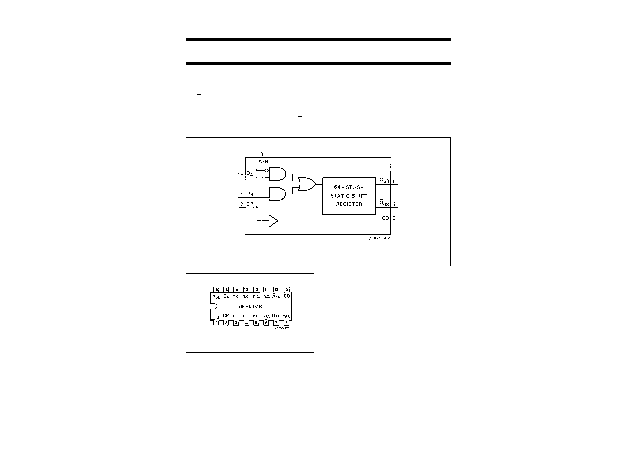
The HEF4031B is an edge-triggered 64-stage static shift
register with two serial data inputs (D
A
, D
B
), a data select
input A/B, a clock input (CP), a buffered clock output (CO),
and buffered outputs from the 64th bit position (O
63
, O
63
).
The output O
63
is capable of driving one TTL load.
Data from D
A
or D
B
, as determined by the state of A/B, is
shifted into the first shift register position and all the data in
the register is shifted one position to the right on the LOW
to HIGH transition of CP. D
A
is selected by a LOW, and D
B
by a HIGH on A/B. Registers can be cascaded either by
connecting all CP inputs together or by driving CP of the
most right-hand register with the system clock and
connecting CO to CP of the preceding register. When the
second technique is used in the recirculating mode, a
flip-flop must be used to store O
63
of the most right-hand
register until the most left-hand register is clocked.
Fig.1 Functional diagram.
HEF4031BP(N):
16-lead DIL; plastic (SOT38-1)
HEF4031BD(F):
16-lead DIL; ceramic (cerdip) (SOT74)
HEF4031BT(D):
16-lead SO; plastic (SOT109-1)
( ): Package Designator North America
Fig.2 Pinning diagram.
PINNING
FAMILY DATA, I
DD
LIMITS category MSI
See Family Specifications
D
A
, D
B
data inputs
A/B
data select input
CP
clock input (LOW to HIGH edge-triggered)
CO
buffered clock output
O
63
buffered output from the 64th stage
O
63
complementary buffered output from the 64th
stage
January 1995
3
Philips Semiconductors
Product specification
64-stage static shift register
HEF4031B
MSI
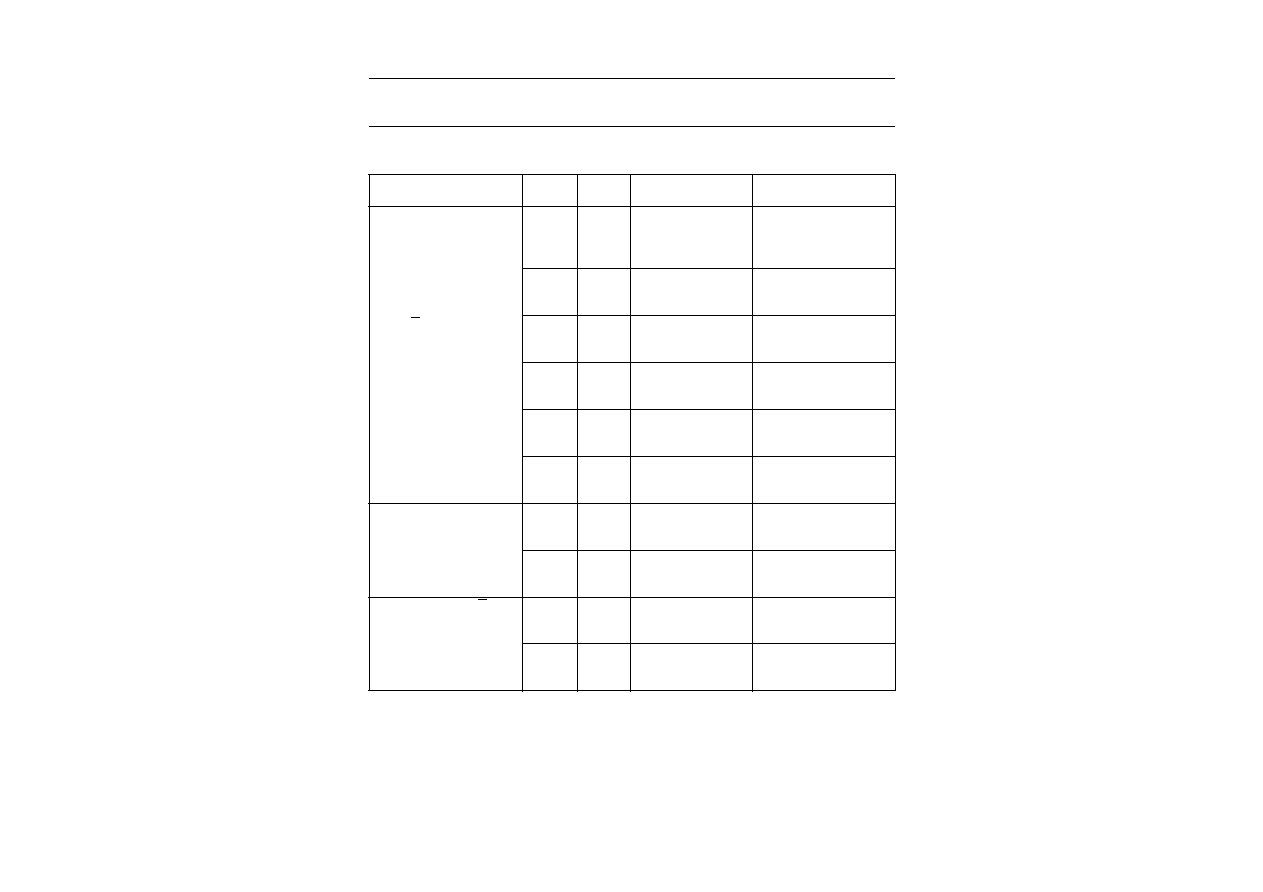
DC CHARACTERISTICS
V
SS
= 0 V; V
I
= V
SS
or V
DD
V
DD
V
V
OH
V
V
OL
V
SYMBOL
T
amb
(
∞
c)
-
40
+
25
+
85
MIN. MAX. MIN.
MAX.
MIN.
MAX.
Output (source)
5
4, 6
1,0
0,85
0,65
mA
current
10
9,5
-
I
OH
3,0
2,5
2,0
mA
HIGH; O
63
15
13,5
10,0
8,5
6,5
mA
HIGH; O
63
5
2,5
-
I
OH
3,0
2,5
2,0
mA
Output (sink)
4,75
0,4
2,7
2,3
1,8
mA
current
10
0,5 I
OL
9,5
8,0
6,3
mA
LOW; O
63
15
1,5
24,0
20,0
16,0
mA
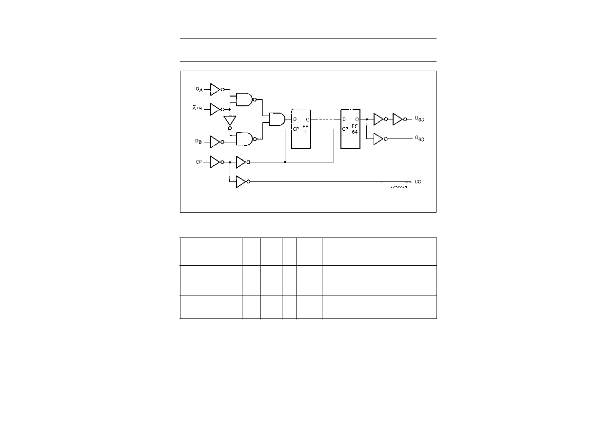
Fig.3 Logic diagram.
January 1995
4
Philips Semiconductors
Product specification
64-stage static shift register
HEF4031B
MSI
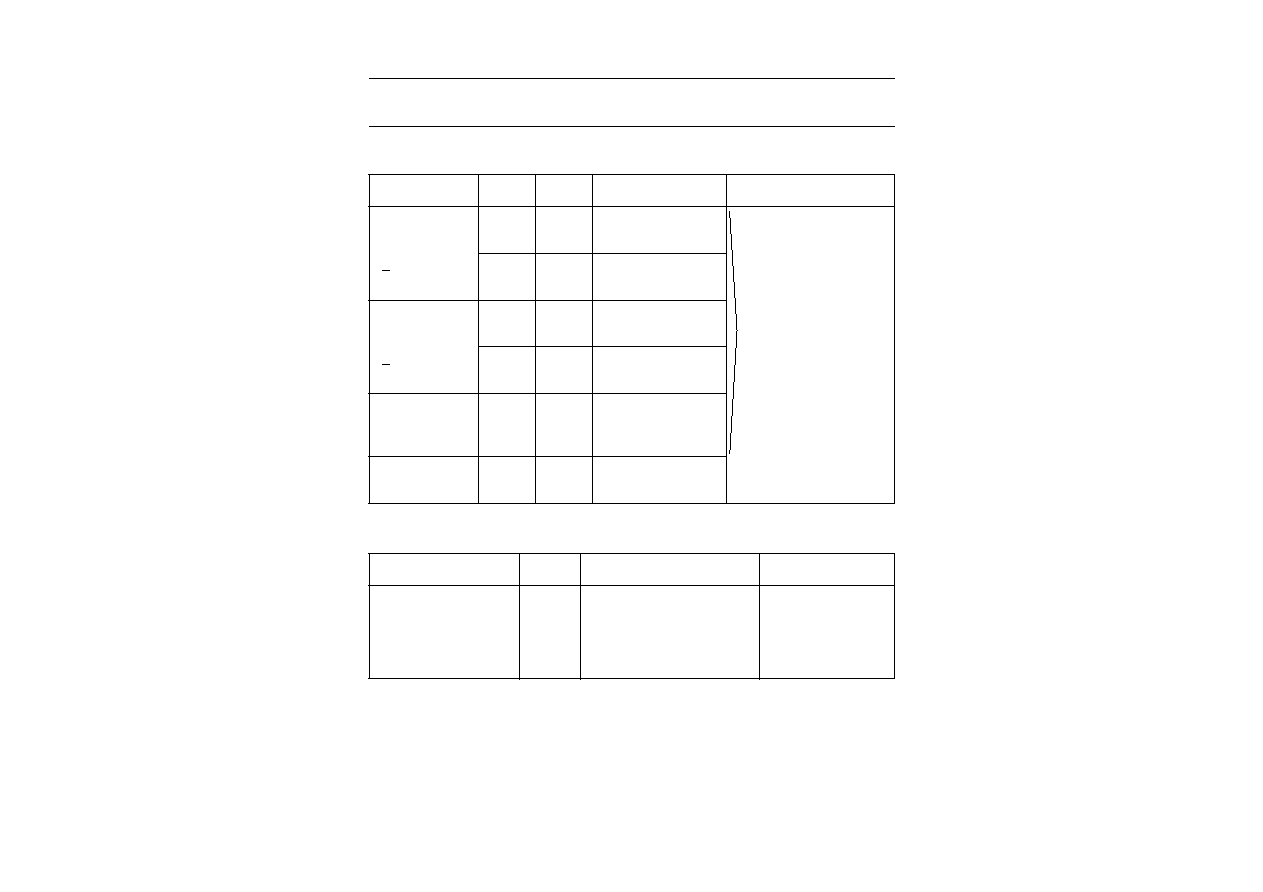
AC CHARACTERISTICS
V
SS
= 0 V; T
amb
= 25
∞
C; C
L
= 50 pF; input transition times
20 ns
V
DD
V
SYMBOL MIN. TYP. MAX.
TYPICAL EXTRAPOLATION
FORMULA
Propagation delays
CP
O
63
5
180
360 ns
167 ns
+
(0,26 ns/pF) C
L
HIGH to LOW
10
t
PHL
65
130 ns
57 ns
+
(0,16 ns/pF) C
L
15
45
90 ns
40 ns
+
(0,11 ns/pF) C
L
5
170
340 ns
148 ns
+
(0,45 ns/pF) C
L
LOW to HIGH
10
t
PLH
65
130 ns
56 ns
+
(0,19 ns/pF) C
L
15
45
90 ns
39 ns
+
(0,13 ns/pF) C
L
CP
O
63
5
190
380 ns
163 ns
+
(0,55 ns/pF) C
L
HIGH to LOW
10
t
PHL
75
150 ns
64 ns
+
(0,23 ns/pF) C
L
15
50
100 ns
42 ns
+
(0,16 ns/pF) C
L
5
190
380 ns
163 ns
+
(0,55 ns/pF) C
L
LOW to HIGH
10
t
PLH
75
150 ns
64 ns
+
(0,23 ns/pF) C
L
15
50
100 ns
42 ns
+
(0,16 ns/pF) C
L
CP
CO
5
70
140 ns
43 ns
+
(0,55 ns/pF) C
L
HIGH to LOW
10
t
PHL
35
70 ns
24 ns
+
(0,23 ns/pF) C
L
15
25
50 ns
17 ns
+
(0,16 ns/pF) C
L
5
55
110 ns
28 ns
+
(0,55 ns/pF) C
L
LOW to HIGH
10
t
PLH
30
60 ns
19 ns
+
(0,23 ns/pF) C
L
15
25
50 ns
17 ns
+
(0,16 ns/pF) C
L
Output transition times;
5
25
50 ns
5 ns
+
(0,40 ns/pF) C
L
O
63
10
t
THL
12
24 ns
3 ns
+
(0,18 ns/pF) C
L
HIGH to LOW
15
8
16 ns
2 ns
+
(0,13 ns/pF) C
L
5
40
80 ns
8 ns
+
(0,65 ns/pF) C
L
LOW to HIGH
10
t
TLH
20
40 ns
5 ns
+
(0,30 ns/pF) C
L
15
13
26 ns
3 ns
+
(0,20 ns/pF) C
L
Output transition times; O
63
, CO
5
60
120 ns
10 ns
+
(1,0 ns/pF) C
L
HIGH to LOW
10
t
THL
30
60 ns
9 ns
+
(0,42 ns/pF) C
L
15
20
40 ns
6 ns
+
(0,28 ns/pF) C
L
5
60
120 ns
10 ns
+
(1,0 ns/pF) C
L
LOW to HIGH
10
t
TLH
30
60 ns
9 ns
+
(0,42 ns/pF) C
L
15
20
40 ns
6 ns
+
(0,28 ns/pF) C
L
January 1995
5
Philips Semiconductors
Product specification
64-stage static shift register
HEF4031B
MSI
AC CHARACTERISTICS
V
SS
= 0 V; T
amb
= 25
∞
C; C
L
= 50 pF; input transition times
20 ns
AC CHARACTERISTICS
V
SS
= 0 V; T
amb
= 25
∞
C; input transition times
20 ns
V
DD
V
SYMBOL
MIN.
TYP. MAX.
TYPICAL EXTRAPOLATION
FORMULA
Set-up times
5
25
0
ns
see also waveforms Fig.4
D
A
, D
B
CP
10
t
su
25
-
5
ns
15
10
-
10
ns
5
30
10
ns
A/B
CP
10
t
su
15
0
ns
15
10
-
5
ns
Hold times
5
40
10
ns
D
A
, D
B
CP
10
t
hold
40
10
ns
15
40
10
ns
5
40
10
ns
A/B
CP
10
t
hold
40
10
ns
15
40
10
ns
Minimum clock
pulse width;
5
180
90
ns
LOW
10
t
WCPL
70
35
ns
15
50
25
ns
Maximum clock
5
2,5
5
MHz
pulse frequency
10
f
max
7
14
MHz
15
10
20
MHz
V
DD
V
TYPICAL FORMULA FOR P (
µ
W)
Dynamic power
5
4000 f
i
+
(f
o
C
L
)
◊
V
DD
2
where
dissipation per
10
19 000 f
i
+
(f
o
C
L
)
◊
V
DD
2
f
i
= input freq. (MHz)
package (P)
15
54 000 f
i
+
(f
o
C
L
)
◊
V
DD
2
f
o
= output freq. (MHz)
C
L
=load capacitance (pF)
(f
o
C
L
) = sum of outputs
V
DD
= supply voltage (V)
January 1995
6
Philips Semiconductors
Product specification
64-stage static shift register
HEF4031B
MSI
APPLICATION INFORMATION
An example of an application for the HEF4031B is:
∑
Serial shift register.
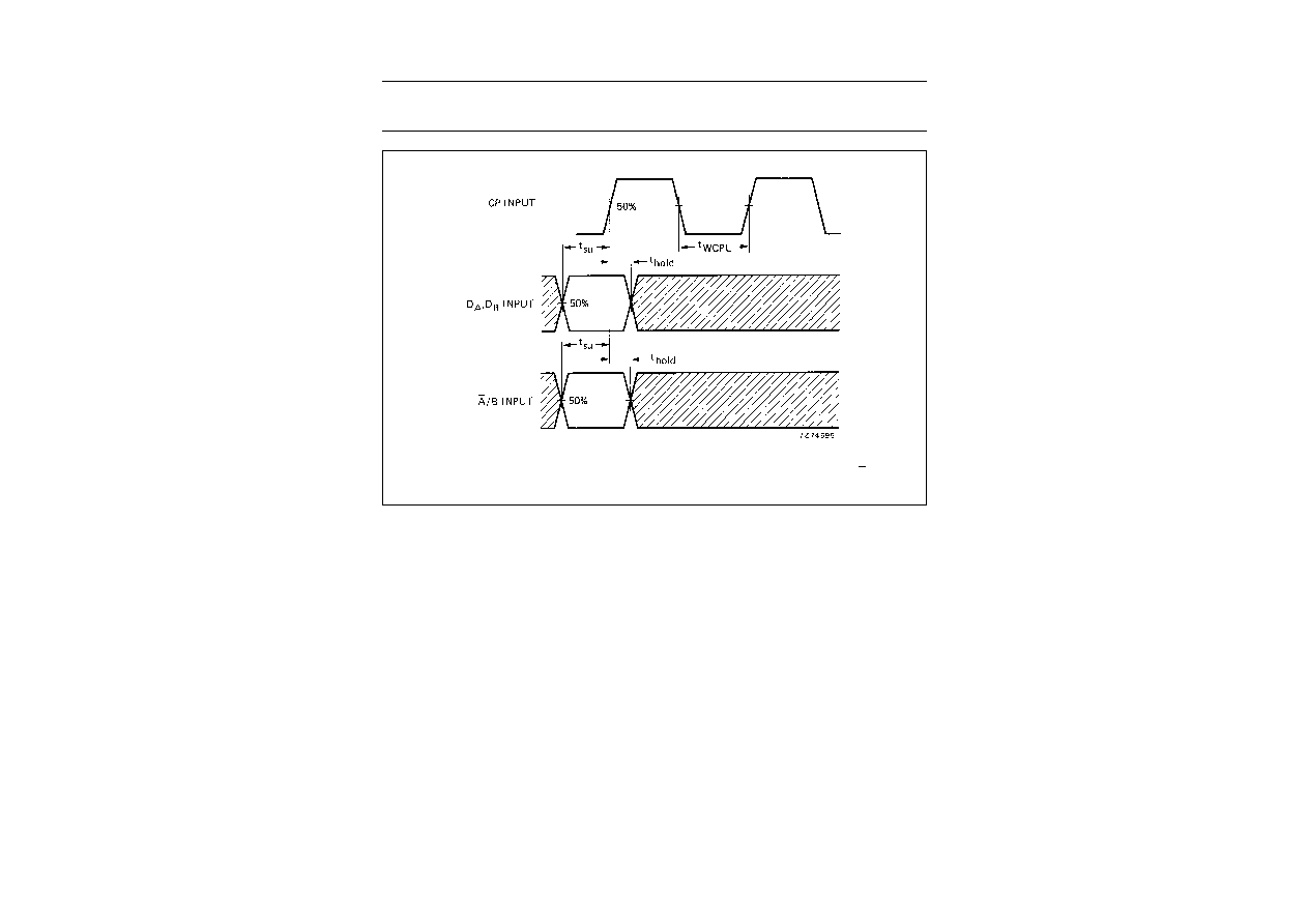
Fig.4
Waveforms showing minimum clock pulse width, set-up and hold times for D
A
, D
B
to CP and A/B to CP.
Set-up and hold times are shown as positive values but may be specified as negative values.
January 1995
7
Philips Semiconductors
Product specification
64-stage static shift register
HEF4031B
MSI
This text is here in white to force landscape pages to be rotated correctly when browsing through the pdf in the Acrobat reader.This text is here in
_
white to force landscape pages to be rotated correctly when browsing through the pdf in the Acrobat reader.This text is here inThis text is here in
white to force landscape pages to be rotated correctly when browsing through the pdf in the Acrobat reader. white to force landscape pages to be ...
APPLICA
TION INFORMA
TION
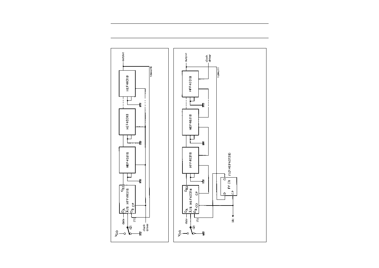
Fig.5 Cascading using direct clocking for high speed operation (see clock rise and fall time requirements).
(1) Recirculating input.
(2) Mode control: V
DD
= recirculation; ground (V
SS
) = new data.
Fig.6 Cascading using delayed clocking for reduced clock drive requirements.
(1) Recirculating input.
(2) Mode control: V
DD
= recirculation; ground (V
SS
) = new data.
(3) For recirculation mode only, FF to delay data until first register delayed clocking has occurred.
(4) Delayed clock-to-clock; new data into first register.