DATA SHEET
Product specification
File under Integrated Circuits, IC04
January 1995
INTEGRATED CIRCUITS
HEF4085B
gates
Dual 2-wide 2-input AND-OR-invert
gate
For a complete data sheet, please also download:
∑
The IC04 LOCMOS HE4000B Logic
Family Specifications HEF, HEC
∑
The IC04 LOCMOS HE4000B Logic
Package Outlines/Information HEF, HEC
January 1995
2
Philips Semiconductors
Product specification
Dual 2-wide 2-input AND-OR-invert gate
HEF4085B
gates
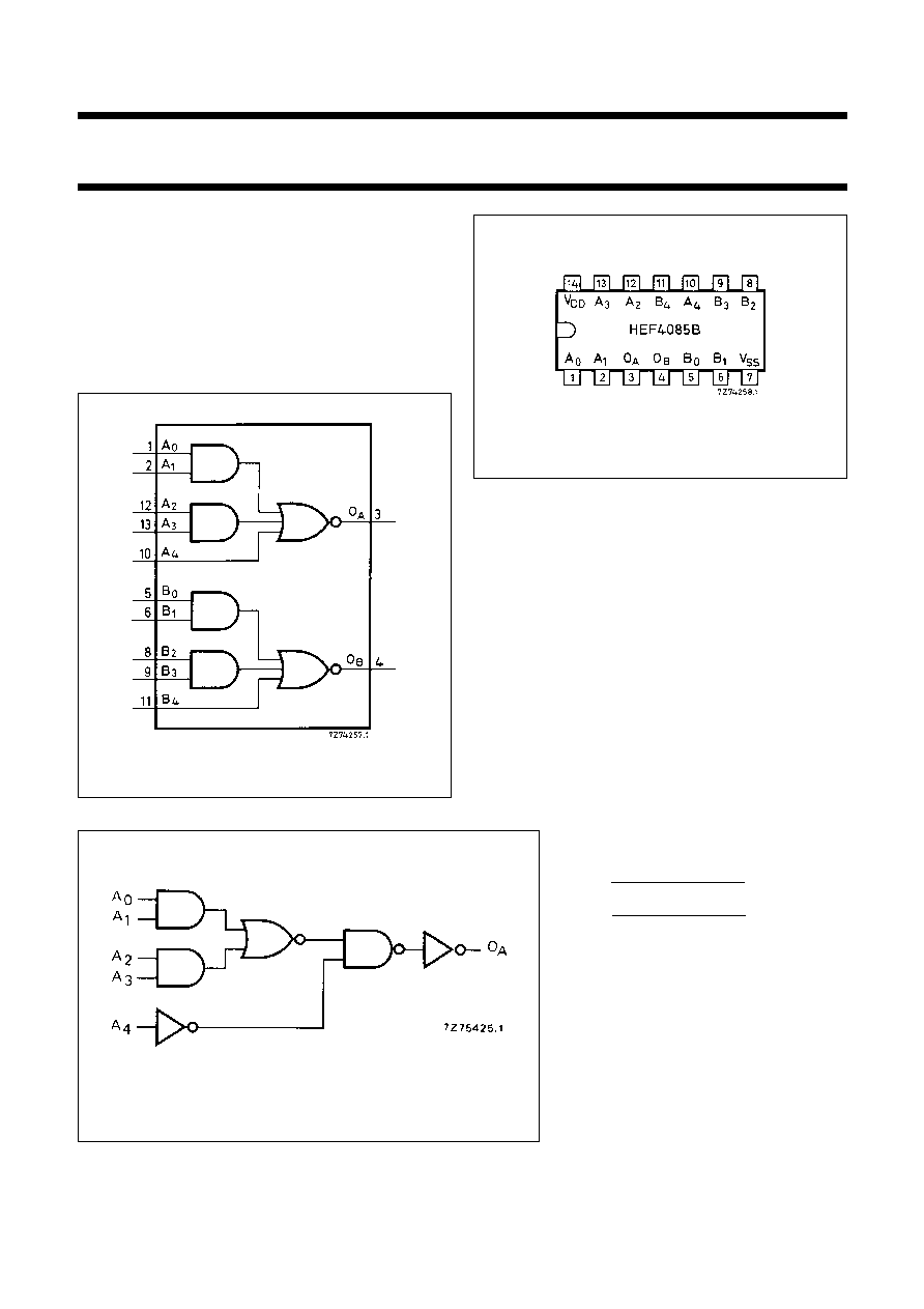
DESCRIPTION
The HEF4085B is a dual 2-wide 2-input AND-OR-invert
gate, each with an additional input (A
4
or B
4
) which can be
used as either an expander input or an inhibit input. A
HIGH on A
4
or B
4
forces the output (O
A
or O
B
) LOW
independent of the other inputs (A
0
to A
3
or B
0
to B
3
). The
outputs O
A
and O
B
are fully buffered for highest noise
immunity and pattern insensitivity of output impedance.
Fig.1 Functional diagram.
HEF4085BP(N): 14-lead DIL; plastic
(SOT27-1)
HEF4085BD(F): 14-lead DIL; ceramic (cerdip)
(SOT73)
HEF4085BT(D): 14-lead SO; plastic
(SOT108-1)
( ): Package Designator North America
Fig.2 Pinning diagram.
Fig.3 Logic diagram (one gate).
LOGIC FUNCTION
FAMILY DATA,
I
DD
LIMITS category GATES
See Family Specifications
O
A
A
0
A
1
A
2
A
3
A
4
+
+
=
O
B
B
0
B
1
B
2
B
3
B
4
+
+
=