 | –≠–ª–µ–∫—Ç—Ä–æ–Ω–Ω—ã–π –∫–æ–º–ø–æ–Ω–µ–Ω—Ç: HEF4086BD | –°–∫–∞—á–∞—Ç—å:  PDF PDF  ZIP ZIP |
Document Outline
- DESCRIPTION
- PINNING
- FAMILY DATA, IDD LIMITS category GATES
- LOGIC EQUATION
- AC CHARACTERISTICS
- APPLICATION INFORMATION

DATA SHEET
Product specification
File under Integrated Circuits, IC04
January 1995
INTEGRATED CIRCUITS
HEF4086B
gates
4-wide 2-input AND-OR-invert gate
For a complete data sheet, please also download:
∑
The IC04 LOCMOS HE4000B Logic
Family Specifications HEF, HEC
∑
The IC04 LOCMOS HE4000B Logic
Package Outlines/Information HEF, HEC
January 1995
2
Philips Semiconductors
Product specification
4-wide 2-input AND-OR-invert gate
HEF4086B
gates
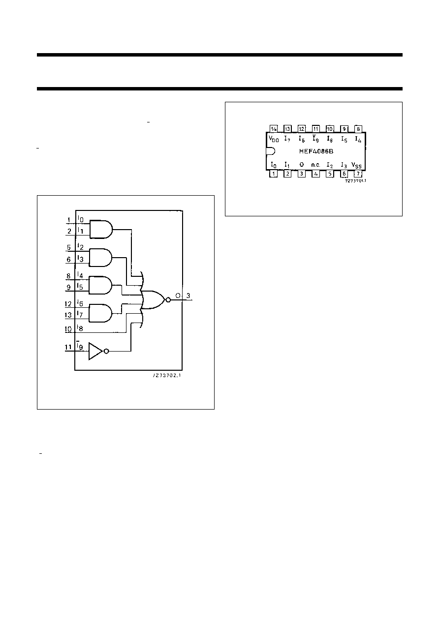
DESCRIPTION
The HEF4086B is a 4-wide 2-input AND-OR-invert (AOI)
gate with two additional inputs (I
8
or I
9
) which can be used
as either expander or inhibit inputs by connecting them to
any standard LOCMOS output. A HIGH on I
8
or a LOW on
I
9
forces the output (O) LOW independent of the other
eight inputs (I
0
to I
7
). The output (O) is fully buffered for
highest noise immunity and pattern insensitivity of output
impedance.
Fig.1 Functional diagram.
HEF4086BP(N): 14-lead DIL; plastic
(SOT27-1)
HEF4086BD(F): 14-lead DIL; ceramic (cerdip)
(SOT73)
HEF4086BT(D): 14-lead SO; plastic
(SOT108-1)
( ): Package Designator North America
Fig.2 Pinning diagram.
PINNING
FAMILY DATA, I
DD
LIMITS category GATES
See Family Specifications
I
0
to I
8
gate inputs
I
9
gate input (active LOW)
O
output (active LOW)
January 1995
3
Philips Semiconductors
Product specification
4-wide 2-input AND-OR-invert gate
HEF4086B
gates
LOGIC EQUATION
Fig.3 Logic diagram.
O
I
0
I
1
I
2
I
3
I
4
I
5
I
6
I
7
I
8
I
9
+
+
+
+
+
=

January 1995
4
Philips Semiconductors
Product specification
4-wide 2-input AND-OR-invert gate
HEF4086B
gates
AC CHARACTERISTICS
V
SS
= 0 V; T
amb
= 25
∞
C; C
L
= 50 pF; input transition times
20 ns
V
DD
V
SYMBOL
TYP.
MAX.
TYPICAL EXTRAPOLATION
FORMULA
Propagation delays
I
0
to I
7
O
5
90
180
ns
63 ns
+
(0,55 ns/pF) C
L
HIGH to LOW
10
t
PHL
30
65
ns
19 ns
+
(0,23 ns/pF) C
L
15
20
40
ns
12 ns
+
(0,16 ns/pF) C
L
5
80
155
ns
53 ns
+
(0,55 ns/pF) C
L
LOW to HIGH
10
t
PLH
30
60
ns
19 ns
+
(0,23 ns/pF) C
L
15
20
40
ns
12 ns
+
(0,16 ns/pF) C
L
I
8
O
5
70
140
ns
43 ns
+
(0,55 ns/pF) C
L
HIGH to LOW
10
t
PHL
25
55
ns
14 ns
+
(0,23 ns/pF) C
L
15
20
40
ns
12 ns
+
(0,16 ns/pF) C
L
5
55
115
ns
28 ns
+
(0,55 ns/pF) C
L
LOW to HIGH
10
t
PLH
20
40
ns
9 ns
+
(0,23 ns/pF) C
L
15
15
25
ns
7 ns
+
(0,16 ns/pF) C
L
I
9
O
5
55
105
ns
28 ns
+
(0,55 ns/pF) C
L
HIGH to LOW
10
t
PHL
20
45
ns
9 ns
+
(0,23 ns/pF) C
L
15
15
30
ns
7 ns
+
(0,16 ns/pF) C
L
5
45
90
ns
18 ns
+
(0,55 ns/pF) C
L
LOW to HIGH
10
t
PLH
15
35
ns
4 ns
+
(0,23 ns/pF) C
L
15
10
25
ns
2 ns
+
(0,16 ns/pF) C
L
Output transition times
5
60
120
ns
10 ns
+
(1,0 ns/pF) C
L
HIGH to LOW
10
t
THL
30
60
ns
9 ns
+
(0,42 ns/pF) C
L
15
20
40
ns
6 ns
+
(0,28 ns/pF) C
L
5
60
120
ns
10 ns
+
(1,0 ns/pF) C
L
LOW to HIGH
10
t
TLH
30
60
ns
9 ns
+
(0,42 ns/pF) C
L
15
20
40
ns
6 ns
+
(0,28 ns/pF) C
L
V
DD
V
TYPICAL FORMULA FOR P (
µ
W)
Dynamic power
5
525 f
i
+
(f
o
C
L
)
◊
V
DD
2
where
dissipation per
10
2600 f
i
+
(f
o
C
L
)
◊
V
DD
2
f
i
= input freq. (MHz)
package (P)
15
7300 f
i
+
(f
o
C
L
)
◊
V
DD
2
f
o
= output freq. (MHz)
C
L
= load capacitance (pF)
(f
o
C
L
) = sum of outputs
V
DD
= supply voltage (V)

January 1995
5
Philips Semiconductors
Product specification
4-wide 2-input AND-OR-invert gate
HEF4086B
gates
APPLICATION INFORMATION
Figure 4 shows two HEF4086B ICs connected to obtain an 8-wide 2-input AOI function.
The output (O
A
) of the first IC is fed directly into the I
9B
gate input of the second IC. Similarly,
any NAND gate output can be fed directly into the I
9
gate input to obtain a 5-wide AOI function.
In addition, any AND gate output can be fed directly into the I
8
gate input with the same result.
Logic equation for Fig.4:
Fig.4 Two HEF4086B ICs connected as an 8-wide 2-input AOI gate.
O
B
I
0A
I
1A
I
2A
I
3A
I
4A
I
5A
I
6A
I
7A
I
0B
I
1B
I
2B
I
3B
I
4B
I
5B
I
6B
I
7B
+
+
+
+
+
+
+
=