 | –≠–ª–µ–∫—Ç—Ä–æ–Ω–Ω—ã–π –∫–æ–º–ø–æ–Ω–µ–Ω—Ç: HEF4508BD | –°–∫–∞—á–∞—Ç—å:  PDF PDF  ZIP ZIP |

DATA SHEET
Product specification
File under Integrated Circuits, IC04
January 1995
INTEGRATED CIRCUITS
HEF4508B
MSI
Dual 4-bit latch
For a complete data sheet, please also download:
∑
The IC04 LOCMOS HE4000B Logic
Family Specifications HEF, HEC
∑
The IC04 LOCMOS HE4000B Logic
Package Outlines/Information HEF, HEC
January 1995
2
Philips Semiconductors
Product specification
Dual 4-bit latch
HEF4508B
MSI
DESCRIPTION
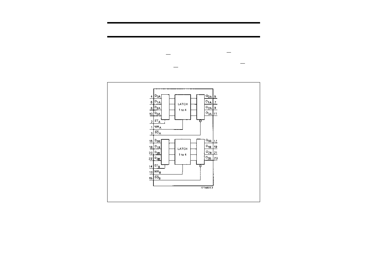
The HEF4508B is a dual 4-bit latch, which consists of two
identical independent 4-bit latches with separate strobe
(ST), master reset (MR), output-enable input (EO) and
3-state outputs (O).
With the ST input in the HIGH state, the data on the D
inputs appear at the corresponding outputs provided EO is
LOW. Changing the ST input to the LOW state locks the
data into the latch. A HIGH on the reset line forces the
outputs to a LOW level regardless of the state of the ST
input. The 3-state outputs are controlled by the
output-enable input. A HIGH on EO causes the outputs to
assume a high impedance OFF-state regardless of other
input conditions. This allows the outputs to interface
directly with bus orientated systems. When EO is LOW the
contents of the latches are available at the outputs.
FAMILY DATA, I
DD
LIMITS category MSI
See Family Specifications
Fig.1 Functional diagram.
January 1995
3
Philips Semiconductors
Product specification
Dual 4-bit latch
HEF4508B
MSI
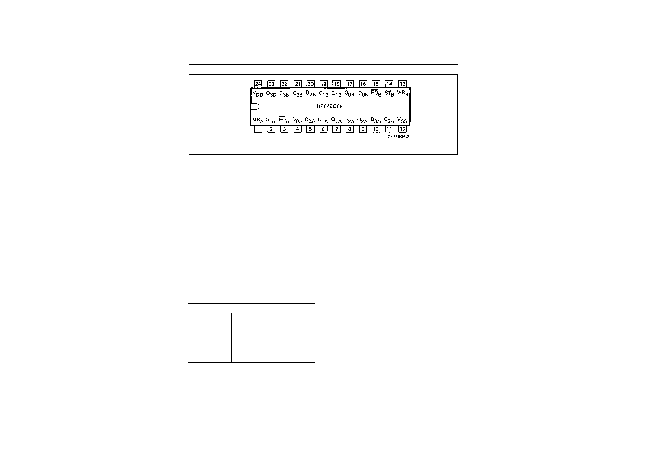
PINNING
FUNCTION TABLE
Notes
1. H = HIGH state (the more positive voltage)
L = LOW state (the less positive voltage)
X = state is immaterial
Z = high impedance OFF state
HEF4508BP(N):
24-lead DIL; plastic
(SOT101-1)
HEF4508BD(F):
24-lead DIL; ceramic (cerdip)
(SOT94)
HEF4508BT(D):
24-lead SO; plastic
(SOT137-1)
( ): Package Designator North America
D
0A
to D
3A
, D
0B
to D
3B
data inputs
ST
A
, ST
B
strobe inputs
MR
A
, MR
B
master reset inputs
EO
A
, EO
B
output enable inputs
O
0A
to O
3A
, O
0B
to O
3B
3-state outputs
INPUTS
OUTPUT
MR
ST
EO
D
n
O
n
L
H
L
H
H
L
H
L
L
L
L
L
L
X
latched
H
X
L
X
L
X
X
H
X
Z
Fig.2 Pinning diagram.

January 1995
4
Philips Semiconductors
Product specification
Dual 4-bit latch
HEF4508B
MSI
Fig.3 Logic diagram (one 4-bit latch).

January 1995
5
Philips Semiconductors
Product specification
Dual 4-bit latch
HEF4508B
MSI
AC CHARACTERISTICS
V
SS
= 0 V; T
amb
= 25
∞
C; C
L
= 50 pF; input transition times
20 ns; see also waveforms Fig.4.
V
DD
V
SYMBOL
MIN.
TYP.
MAX.
TYPICAL EXTRAPOLATION
FORMULA
Propagation delays
ST
O
n
5
115
230
ns
88 ns
+
(0,55 ns/pF) C
L
HIGH to LOW
10
t
PHL
50
100
ns
39 ns
+
(0,23 ns/pF) C
L
15
35
70
ns
27 ns
+
(0,16 ns/pF) C
L
5
115
230
ns
88 ns
+
(0,55 ns/pF) C
L
LOW to HIGH
10
t
PLH
50
100
ns
39 ns
+
(0,23 ns/pF) C
L
15
35
70
ns
27 ns
+
(0,16 ns/pF) C
L
D
n
O
n
5
95
190
ns
68 ns
+
(0,55 ns/pF) C
L
HIGH to LOW
10
t
PHL
40
80
ns
29 ns
+
(0,23 ns/pF) C
L
15
30
60
ns
22 ns
+
(0,16 ns/pF) C
L
5
95
190
ns
68 ns
+
(0,55 ns/pF) C
L
LOW to HIGH
10
t
PLH
40
80
ns
29 ns
+
(0,23 ns/pF) C
L
15
30
60
ns
22 ns
+
(0,16 ns/pF) C
L
MR
O
n
5
100
200
ns
73 ns
+
(0,55 ns/pF) C
L
HIGH to LOW
10
t
PHL
40
80
ns
29 ns
+
(0,23 ns/pF) C
L
15
30
60
ns
22 ns
+
(0,16 ns/pF) C
L
Output transition times
5
60
120
ns
10 ns
+
(1,0 ns/pF) C
L
HIGH to LOW
10
t
THL
30
60
ns
9 ns
+
(0,42 ns/pF) C
L
15
20
40
ns
6 ns
+
(0,28 ns/pF) C
L
5
60
120
ns
10 ns
+
(1,0 ns/pF) C
L
LOW to HIGH
10
t
TLH
30
60
ns
9 ns
+
(0,42 ns/pF) C
L
15
20
40
ns
6 ns
+
(0,28 ns/pF) C
L
3-state propagation
delays
Output enable times
EO
O
n
5
45
90
ns
HIGH
10
t
PZH
20
40
ns
15
18
36
ns
5
45
90
ns
LOW
10
t
PZL
20
40
ns
15
18
36
ns
Output disable times
EO
O
n
5
35
70
ns
HIGH
10
t
PHZ
20
40
ns
15
18
36
ns
5
45
90
ns
LOW
10
t
PLZ
20
40
ns
15
18
36
ns

January 1995
6
Philips Semiconductors
Product specification
Dual 4-bit latch
HEF4508B
MSI
AC CHARACTERISTICS
V
SS
= 0 V; T
amb
= 25
∞
C; C
L
= 50 pF; input transition times
20 ns
V
DD
V
SYMBOL
MIN. TYP.
MAX.
Minimum ST
5
50
25
ns
see also waveforms Fig.4
pulse width; HIGH
10
t
WSTH
30
15
ns
15
20
10
ns
Minimum MR pulse
5
40
20
ns
width; HIGH
10
t
WMRH
24
12
ns
15
20
10
ns
Recovery time
5
20
0
ns
for MR
10
t
RMR
20
0
ns
15
15
0
ns
Set-up times
5
35
10
ns
D
n
ST
10
t
su
25
5
ns
15
20
0
ns
Hold times
5
20
0
ns
D
n
ST
10
t
hold
20
0
ns
15
15
0
ns
V
DD
V
TYPICAL FORMULA FOR P (
µ
W)
Dynamic power
5
2 000 f
i
+
(f
o
C
L
)
◊
V
DD
2
where
dissipation per
10
9 000 f
i
+
(f
o
C
L
)
◊
V
DD
2
f
i
= input freq. (MHz)
package (P)
15
25 000 f
i
+
(f
o
C
L
)
◊
V
DD
2
f
o
= output freq. (MHz)
C
L
= load capacitance (pF)
(f
o
C
L
) = sum of outputs
V
DD
= supply voltage (V)

January 1995
7
Philips Semiconductors
Product specification
Dual 4-bit latch
HEF4508B
MSI
This text is here in white to force landscape pages to be rotated correctly when browsing through the pdf in the Acrobat reader.This text is here in
_
white to force landscape pages to be rotated correctly when browsing through the pdf in the Acrobat reader.This text is here inThis text is here in
white to force landscape pages to be rotated correctly when browsing through the pdf in the Acrobat reader. white to force landscape pages to be ...
Fig.4
Waveforms showing minimum ST and MR pulse widths, set-up and hold times for D
n
to ST, recovery time for MR and propagation
delays from ST to O
n
, to D
n
to O
n
and MR to O
n
.

January 1995
8
Philips Semiconductors
Product specification
Dual 4-bit latch
HEF4508B
MSI
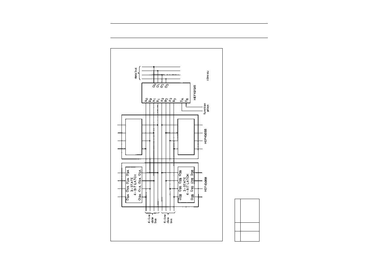
APPLICATION INFORMATION
Some examples of application for the HEF4508B are:
∑
Buffer storage
∑
Holding registers
∑
Data storage and multiplexing
Fig.5 Example of a bus register using HEF4508B and HEF4015B.
January 1995
9
Philips Semiconductors
Product specification
Dual 4-bit latch
HEF4508B
MSI
This text is here in white to force landscape pages to be rotated correctly when browsing through the pdf in the Acrobat reader.This text is here in
_
white to force landscape pages to be rotated correctly when browsing through the pdf in the Acrobat reader.This text is here inThis text is here in
white to force landscape pages to be rotated correctly when browsing through the pdf in the Acrobat reader. white to force landscape pages to be ...
FUNCTION SELECT
S
A
S
B
FUNCTION
L
L
inhibit (all L)
H
L
select A bus
L
H
select B bus
H
H
A
1
+
B
1
Fig.6 Example of a dual multiplexed bus register with function select using two HEF4508B and one HEF4019B.