DATA SHEET
Product specification
File under Integrated Circuits, IC04
January 1995
INTEGRATED CIRCUITS
HEF4528B
MSI
Dual monostable multivibrator
For a complete data sheet, please also download:
∑
The IC04 LOCMOS HE4000B Logic
Family Specifications HEF, HEC
∑
The IC04 LOCMOS HE4000B Logic
Package Outlines/Information HEF, HEC

January 1995
2
Philips Semiconductors
Product specification
Dual monostable multivibrator
HEF4528B
MSI
DESCRIPTION
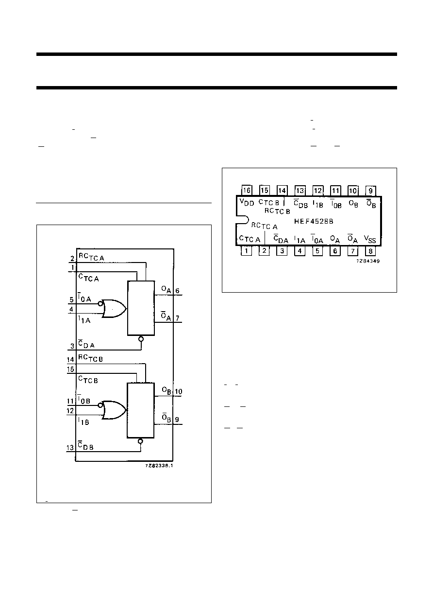
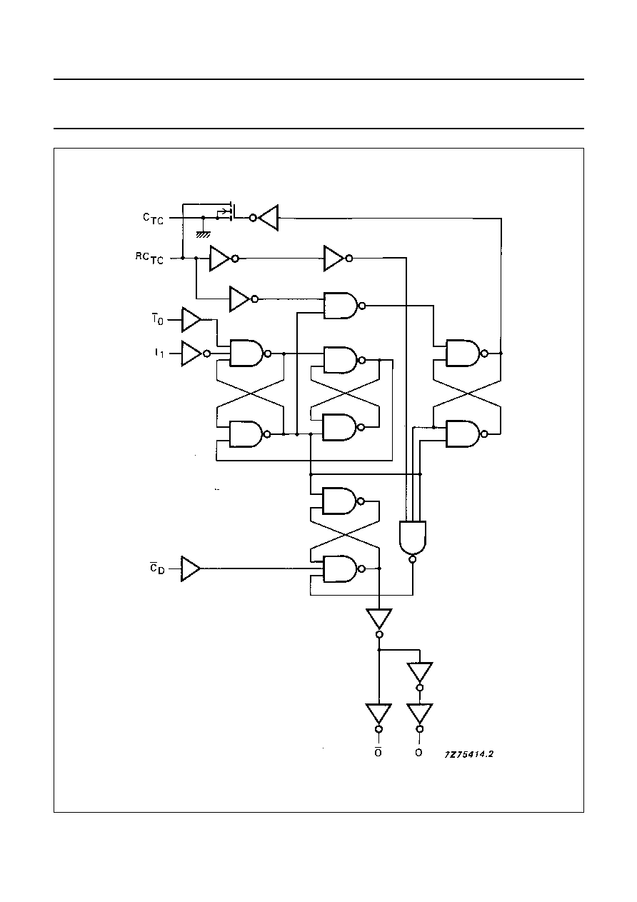
The HEF4528B is a dual retriggerable-resettable
monostable multivibrator. Each multivibrator has an active
LOW input (I
0
), and active HIGH input (I
1
), an active LOW
clear direct input (C
D
), an output (O) and its complement
(O), and two pins for connecting the external timing
components (C
TC
(1)
, RC
TC
).
An external timing capacitor (C
t
) must be connected
between C
TC
and RC
TC
and an external resistor (R
t
) must
be connected between RC
TC
and V
DD
. The duration of the
(1) Always connected to ground.
output pulse is determined by the external timing
components C
t
and R
t
.
A HIGH to LOW transition on I
0
when I
1
is LOW or a LOW
to HIGH transition on I
1
when I
0
is HIGH produces a
positive pulse (LOW-HIGH-LOW) and O and a negative
pulse (HIGH-LOW-HIGH) on O if the C
D
is HIGH. A LOW
on C
D
forces O LOW, O HIGH and inhibits any further
pulses until C
D
is HIGH.
Fig.1 Functional diagram.
PINNING
FAMILY DATA, I
DD
LIMITS category MSI
See Family Specifications
HEF4528BP(N):
16-lead DIL; plastic (SOT38-1)
HEF4528BD(F):
16-lead DIL; ceramic (cerdip) (SOT74)
HEF4528BT(D):
16-lead SO; plastic (SOT109-1)
( ): Package Designator North America
I
0A,
I
0B
input (HIGH to LOW triggered)
I
1A
, I
1B
input (LOW to HIGH triggered)
C
DA
, C
DB
clear direct input (active LOW)
O
A
, O
B
output
O
A
, O
B
complementary output (active LOW)
C
TC A
, C
TC B
external capacitor connections
(1)
RC
TC A
,
external capacitor/ resistor connections
RC
TC B
Fig.2 Pinning diagram.

January 1995
4
Philips Semiconductors
Product specification
Dual monostable multivibrator
HEF4528B
MSI
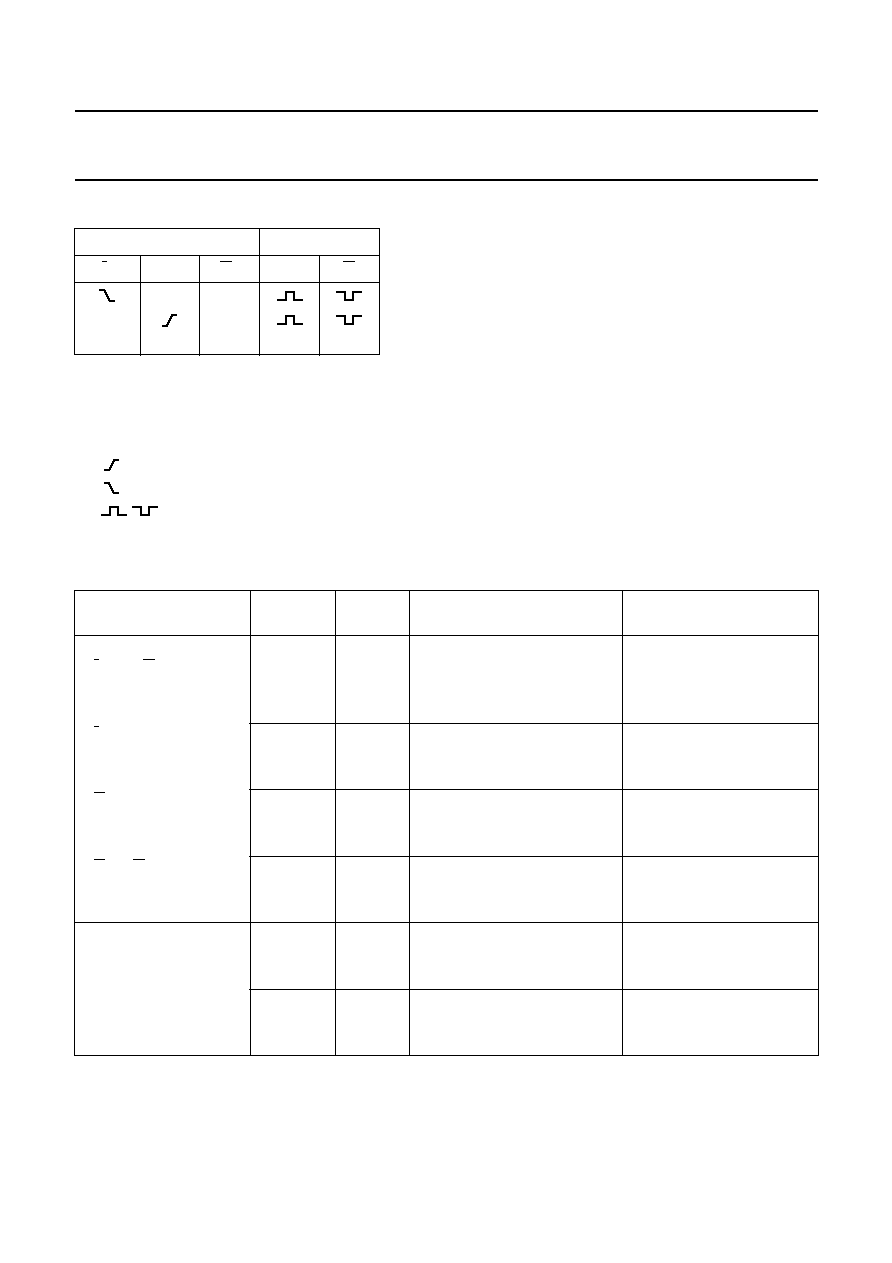
FUNCTION TABLE
Notes
1. H = HIGH state (the more positive voltage)
2. L = LOW state (the less positive voltage)
3. X = state is immaterial
4.
= positive-going transition
5.
= negative-going transition
6.
= positive or negative output pulse; width is determined by C
t
and R
t
AC CHARACTERISTICS
V
SS
= 0 V; T
amb
= 25
∞
C; C
L
= 50 pF; input transition times
20 ns
INPUTS
OUTPUTS
I
0
I
1
C
D
O
O
L
H
H
H
X
X
L
L
H
V
DD
V
SYMBOL
MIN.
TYP.
MAX.
TYPICAL EXTRAPOLATION
FORMULA
Propagation delays
I
0
, I
1
O
5
140
280
ns
113 ns
+
(0,55 ns/pF) C
L
HIGH to LOW
10
t
PHL
50
100
ns
39 ns
+
(0,23 ns/pF) C
L
15
35
70
ns
27 ns
+
(0,16 ns/pF) C
L
I
0
, I
1
O
5
155
305
ns
128 ns
+
(0,55 ns/pF) C
L
LOW to HIGH
10
t
PLH
60
115
ns
49 ns
+
(0,23 ns/pF) C
L
15
40
80
ns
32 ns
+
(0,16 ns/pF) C
L
C
D
O
5
105
210
ns
78 ns
+
(0,55 ns/pF) C
L
HIGH to LOW
10
t
PHL
40
85
ns
29 ns
+
(0,23 ns/pF) C
L
15
30
60
ns
22 ns
+
(0,16 ns/pF) C
L
C
D
O
5
120
240
ns
93 ns
+
(0,55 ns/pF) C
L
LOW to HIGH
10
t
PLH
50
105
ns
39 ns
+
(0,23 ns/pF) C
L
15
35
70
ns
27 ns
+
(0,16 ns/pF) C
L
Output transition
5
60
120
ns
10 ns
+
(1,0 ns/pF) C
L
times
10
t
THL
30
60
ns
9 ns
+
(0,42 ns/pF) C
L
HIGH to LOW
15
20
40
ns
6 ns
+
(0,28 ns/pF) C
L
5
60
120
ns
10 ns
+
(1,0 ns/pF) C
L
LOW to HIGH
10
t
TLH
30
60
ns
9 ns
+
(0,42 ns/pF) C
L
15
20
40
ns
6 ns
+
(0,28 ns/pF) C
L

January 1995
5
Philips Semiconductors
Product specification
Dual monostable multivibrator
HEF4528B
MSI
AC CHARACTERISTICS
V
SS
= 0 V; T
amb
= 25
∞
C; input transition times
20 ns; R
t
= 5 k
; C
t
= 15 pF
AC CHARACTERISTICS
V
SS
= 0 V; T
amb
= 25
∞
C; C
L
= 50 pF; input transition times
20 ns; see also waveforms Fig.5.
V
DD
V
TYPICAL FORMULA FOR P (
µ
W)
Dynamic power
5
4000 f
i
+
(f
o
C
L
)
◊
V
DD
2
where
dissipation per
10
20 000 f
i
+
(f
o
C
L
)
◊
V
DD
2
f
i
= input freq. (MHz)
package (P)
15
59 000 f
i
+
(f
o
C
L
)
◊
V
DD
2
f
o
= output freq. (MHz)
C
L
= load capacitance (pF)
(f
o
C
L
) = sum of outputs
V
DD
= supply voltage (V)
V
DD
V
SYMBOL
MIN.
TYP.
MAX.
Recovery time
5
0
-
75
ns
for C
D
10
t
RCD
0
-
30
ns
15
0
-
25
ns
Minimum I
0
5
50
25
ns
pulse width; LOW
10
t
WI0L
30
15
ns
15
20
10
ns
Minimum I
1
5
50
25
ns
pulse width; HIGH
10
t
WI1H
30
15
ns
15
20
10
ns
Minimum C
D
5
60
30
ns
pulse width; LOW
10
t
WCDL
35
15
ns
15
25
10
ns
Set-up time
5
0
-
105
ns
to avoid change
in output
C
D
I
0
or I
1
10
t
su
0
-
40
ns
15
0
-
25
ns
Output O pulse
5
-
235
ns
note 1
width; HIGH
10
t
WOH
-
155
ns
15
-
140
ns
Output O pulse
5
-
5,45
µ
s
note 2
width; HIGH
10
t
WOH
-
4,95
µ
s
15
-
4,85
µ
s
Change in output O
5
-
±
3
%
note 3
pulse width over
10
t
WO
-
±
2
%
temperature
15
-
±
2
%
Change in output O
5
-
±
2
%
V
DD
±
5%
pulse width over
10
t
WO
-
±
1
%
V
DD
15
-
±
1
%

