 | –≠–ª–µ–∫—Ç—Ä–æ–Ω–Ω—ã–π –∫–æ–º–ø–æ–Ω–µ–Ω—Ç: HEF4731BF | –°–∫–∞—á–∞—Ç—å:  PDF PDF  ZIP ZIP |
Document Outline
- DESCRIPTION
- FAMILY DATA, IDD LIMITS category LSI
- DC CHARACTERISTICS
- AC CHARACTERISTICS
- AC CHARACTERISTICS
DATA SHEET
Product specification
File under Integrated Circuits, IC04
January 1995
INTEGRATED CIRCUITS
HEF4731B; HEF4731V
LSI
Quadruple 64-bit static shift register
For a complete data sheet, please also download:
∑
The IC04 LOCMOS HE4000B Logic
Family Specifications HEF, HEC
∑
The IC04 LOCMOS HE4000B Logic
Package Outlines/Information HEF, HEC
January 1995
2
Philips Semiconductors
Product specification
Quadruple 64-bit static shift register
HEF4731B; HEF4731V
LSI
DESCRIPTION
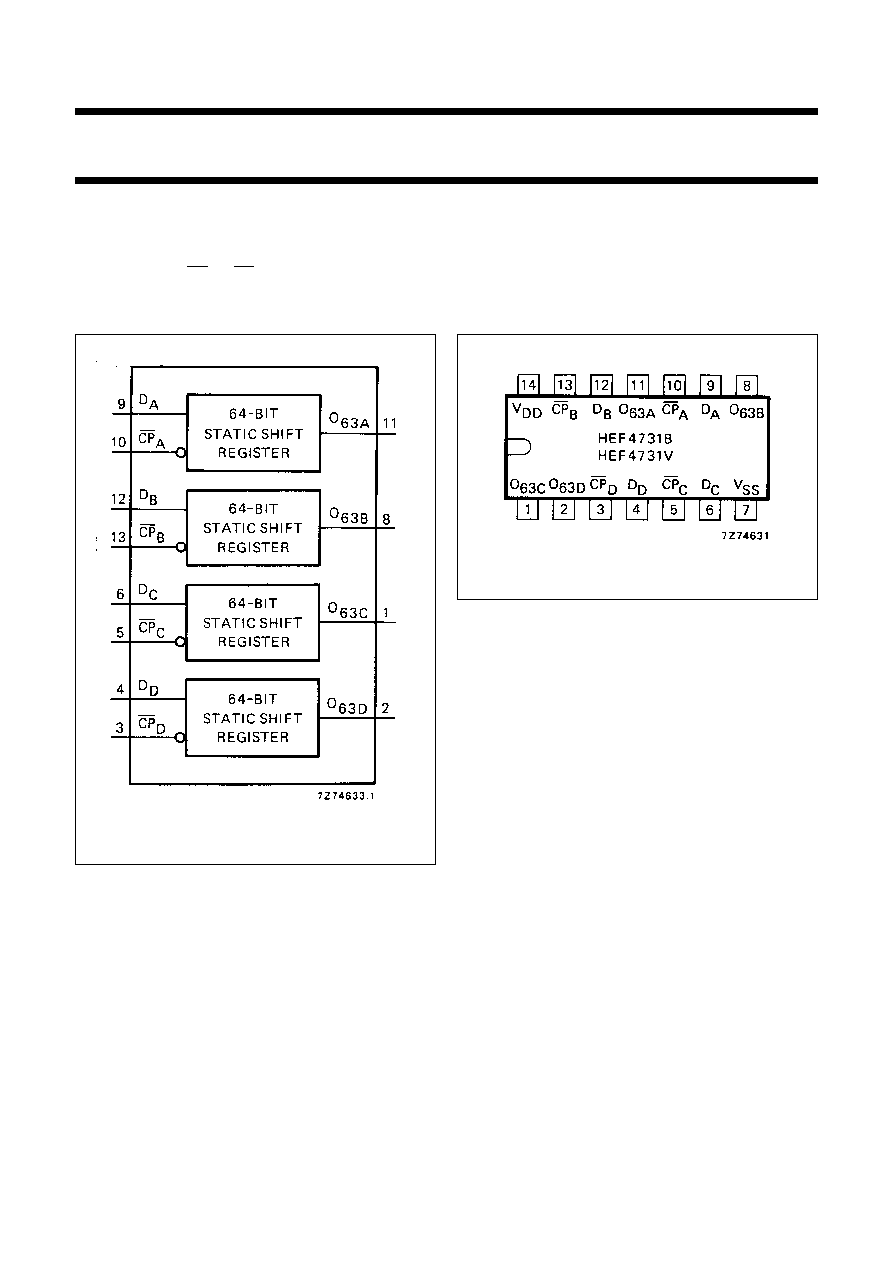
The HEF4731B and HEF4731V are quadruple 64-bit static
shift registers each with separate serial data inputs (D
A
to
D
D
), clock inputs (CP
A
to CP
D
) and data outputs (O
63A
to
O
63D
) from the 64th register position.
Recommended supply voltage range for HEF4731B is 3 to
15 V and for HEF4731V is 4,5 to 12,5 V.
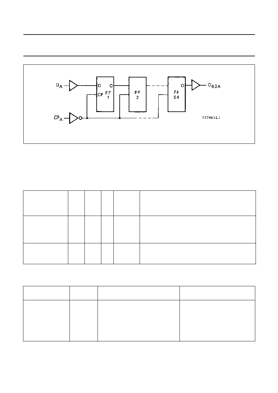
Data are shifted to the next stage on the negative-going
transitions of the clock. Low impedance outputs are
provided for direct interface to TTL.
Fig.1 Functional diagram.
FAMILY DATA, I
DD
LIMITS category LSI
See Family Specifications
HEF4731BP;
HEF4731VP(N):
14-lead DIL; plastic
(SOT27-1)
HEF4731BD;
HEF4731VD(F):
14-lead DIL; ceramic (cerdip)
(SOT73)
( ): Package Designator North America
Fig.2 Pinning diagram.
January 1995
3
Philips Semiconductors
Product specification
Quadruple 64-bit static shift register
HEF4731B; HEF4731V
LSI
The values given at V
DD
= 15 V in the following DC
and AC characteristics, are not applicable to the HEF4731V,
because of its reduced supply voltage range.
DC CHARACTERISTICS
V
SS
= 0 V; V
I
= V
SS
or V
DD
AC CHARACTERISTICS
V
SS
= 0 V; T
amb
= 25
∞
C; input transition times
20 ns
V
DD
V
V
OL
V
V
OH
V
SYMBOL
T
amb
(
∞
C)
-
40
+
25
+
85
MIN.
MAX.
MIN.
MAX.
MIN.
MAX.
Output (source)
5
2,5
3
2,5
2,0
mA
current
5
4,6
-
I
OH
1
0,85
0,65
mA
HIGH
10
9,5
3
2,5
2,0
mA
15
13,5
10
8,5
6,5
mA
Output (sink)
4,75
0,4
2,3
2,0
1,6
mA
current
10
0,5
I
OL
6,0
5,0
4,0
mA
LOW
15
1,5
20,0
18,0
14,0
mA
V
DD
V
TYPICAL FORMULA FOR P (
µ
W)
Dynamic power
5
13 000 f
i
+
(f
o
C
L
)
◊
V
DD
2
where
dissipation per
10
55 000 f
i
+
(f
o
C
L
)
◊
V
DD
2
f
i
= input freq. (MHz)
package (P)
15
140 000 f
i
+
(f
o
C
L
)
◊
V
DD
2
f
o
= output freq. (MHz)
C
L
= load capacitance (pF)
(f
o
C
L
) = sum of outputs
V
DD
= supply voltage (V)
Fig.3 Logic diagram (one of 64-bits shift register).
January 1995
4
Philips Semiconductors
Product specification
Quadruple 64-bit static shift register
HEF4731B; HEF4731V
LSI
AC CHARACTERISTICS
V
SS
= 0 V; T
amb
= 25
∞
C; C
L
= 50 pF; input transition times
20 ns
V
DD
V
SYMBOL
MIN.
TYP.
MAX.
TYPICAL EXTRAPOLATION
FORMULA
Propagation delays
CP
O
63
5
115
230 ns
132 ns
+
(0,26 ns/pF) C
L
HIGH to LOW
10
t
PHL
55
110 ns
47 ns
+
(0,16 ns/pF) C
L
15
40
80 ns
34 ns
+
(0,11 ns/pF) C
L
5
130
260 ns
138 ns
+
(0,45 ns/pF) C
L
LOW to HIGH
10
t
PLH
65
130 ns
56 ns
+
(0,19 ns/pF) C
L
15
45
90 ns
39 ns
+
(0,13 ns/pF) C
L
Transition times O
63
5
30
60 ns
10 ns
+
(0,40 ns/pF) C
L
HIGH to LOW
10
t
THL
12
24 ns
3 ns
+
(0,18 ns/pF) C
L
15
10
20 ns
3 ns
+
(0,13 ns/pF) C
L
5
40
80 ns
8 ns
+
(0,65 ns/pF) C
L
LOW to HIGH
10
t
TLH
20
40 ns
5 ns
+
(0,30 ns/pF) C
L
15
15
30 ns
5 ns
+
(0,20 ns/pF) C
L
Minimum clock
5
200
80
ns
see also waveforms Fig.4
pulse width; HIGH
10
t
WCPH
75
30
ns
15
50
20
ns
Set-up time
5
25
-
5
ns
D
CP
10
t
su
15
-
5
ns
15
15
-
5
ns
Hold time
5
50
20
ns
D
CP
10
t
hold
30
10
ns
15
20
5
ns
Maximum clock
5
2.25
6
MHz
Note: the maximum
pulse frequency
10
f
max
6
16
MHz
power dissipation has
15
9
25
MHz
to be observed
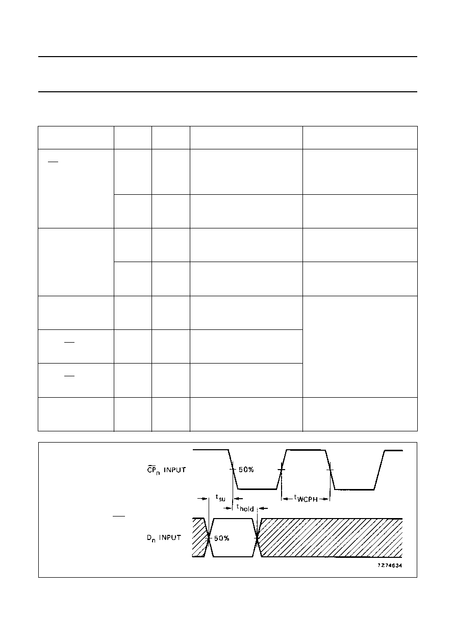
Fig.4
Waveforms showing
minimum clock pulse
width, set-up and hold
times for D to CP.
Set-up and hold times
are shown as positive
values but may be
specified as negative
values.