 | ÐлекÑÑоннÑй компоненÑ: HEF4755VT | СкаÑаÑÑ:  PDF PDF  ZIP ZIP |
Äîêóìåíòàöèÿ è îïèñàíèÿ www.docs.chipfind.ru

DATA SHEET
Product specification
File under Integrated Circuits, IC04
January 1995
INTEGRATED CIRCUITS
HEF4755V
LSI
Transceiver for serial data
communication
For a complete data sheet, please also download:
·
The IC04 LOCMOS HE4000B Logic
Family Specifications HEF, HEC
·
The IC04 LOCMOS HE4000B Logic
Package Outlines/Information HEF, HEC
January 1995
2
Philips Semiconductors
Product specification
Transceiver for serial data communication
HEF4755V
LSI
DESCRIPTION
The HEF4755V transceiver is a circuit for serial data
communication. It provides maximum transmission
security and effectiveness. Therefore, in addition to the
normal precautions, it contains a programmable digital
bit-check, a programmable CRC (Cyclic Redundancy
Check; Hamming distance 4 or 6) and format protection.
The circuit has 8 possible operating modes:
·
synchronous
error checking only
receiving
transmitting
receiving with data out and transmitting the same
message
·
asynchronous
error checking only
receiving
transmitting
receiving with data out and transmitting of a
regenerated message.
FEATURES
·
Transmission rate:
·
Inputs: standard LOCMOS
·
Outputs: TTL compatible (1 TTL load)
·
Operating ambient temperature range:
-
40 to
+
85
°
C
·
Transmit or receive a serial binary data stream
·
Start bit generation and recognition
·
Format protection and checking
·
Redundancy byte generation and checking
·
Digital bit check
·
Error recognition and error distinguishing
·
8-bit parallel input/output transfer
V
DD
SYNCHRONOUS
ASYNCHRONOUS
5 V
0,8 Mbaud
31 kbaud
7 V
1,6 Mbaud
62 kbaud
10 V
3,2 Mbaud
125 kbaud
SUPPLY VOLTAGE/CURRENT
FAMILY DATA, I
DD
LIMITS category LSI
See Family Specification
RATING
RECOMMENDED OPERATING
V
DD
-
0,5 to
+
15
4,75 to 12,6
V
I
SS
30
-
mA
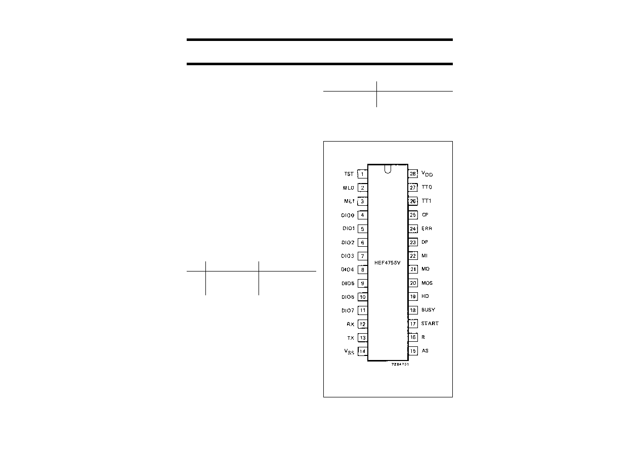
Fig.1 Pinning diagram.

January 1995
3
Philips Semiconductors
Product specification
Transceiver for serial data communication
HEF4755V
LSI
HEF4755VP(N):
28-lead DIL; plastic
(SOT117-2)
HEF4755VD(F):
28-lead DIL; ceramic (cerdip)
(SOT135)
HEF4755VT(D):
28-lead SO; plastic
(SOT136-1)
( ): Package Designator North America
PINNING
1
TST
Test pin; during normal use
connected to V
SS
. When TST is
HIGH (V
DD
), internal check points
are connected to the data bus.
2
ML0
Input code for message length (see
Table 1).
3
ML1
4
DIO0
Bidirectional data bus.
to
to
11
DIO7
12
RX
Mode input: receive; see Table 2
13
TX
Mode input: transmit; see Table 2
15
AS
Mode input: asynchronous;
see Table 2
16
R
Reset; a positive signal resets
all internal registers.
17
START
Input start in transmitting mode;
synchronization input (from MOS)
in synchronous receiving mode.
18
BUSY
Output busy; active during
receiving or transmitting a message.
19
HD
Hamming distance; determines the
length of the redundancy byte:
LOW = 7 bit (HD = 4)
HIGH = 15 bit (HD = 6)
20
MOS
Output message synchronization
used in synchronous mode.
21
MO
Message output.
22
MI
Message input.
23
DP
Output data pulse; take-over pulse
for data on the data bus.
24
ERR
Output error; an active output
means that at least 1 transmission
error is recognized.
25
CP
Clock input; in synchronous mode
equal to the transmission bit rate.
26
TT1
Programming of the permissible time
tolerance in bit distortion
(see Table 3).
27
TT0
28
V
DD
Positive supply voltage; 4,5 V to
12,5 V (is the logic HIGH level).
14
V
SS
Ground (is the logic LOW level).
January 1995
4
Philips Semiconductors
Product specification
Transceiver for serial data communication
HEF4755V
LSI
Table 1
Input code for message length
Table 2
Input code for input mode
Table 3
Permissible time tolerance in bit distortion
Notes
1. H = HIGH state (the most positive voltage)
2. L = LOW state (the least positive voltage)
ML0
ML1
MESSAGE LENGTH
H
H
6 data bytes
L
H
4 data bytes
H
L
2 data bytes
L
L
variable length
depends on
format byte
RX
TX
AS
L
L
L
status register connected to the data bus for error recognition
H
L
L
receiving in synchronous mode
L
H
L
transmitting in synchronous mode
H
H
L
receiving messages (without redundancy bit); data parallel out;
calculating of redundancy byte; transmitting data with redundancy
byte in synchronous mode
L
L
H
only bit check in asynchronous mode; no data output on data bus
H
L
H
receiving in asynchronous mode
L
H
H
transmitting in asynchronous mode
H
H
H
receiving and transmitting of a regenerated message in the
asynchronous mode
TT1
TT0
PERMITTED DISTORTION (dt/T)
L
L
6/32
19%
L
H
8/32 = 25%
H
L
10/32
31%
H
H
12/32
37%
January 1995
5
Philips Semiconductors
Product specification
Transceiver for serial data communication
HEF4755V
LSI
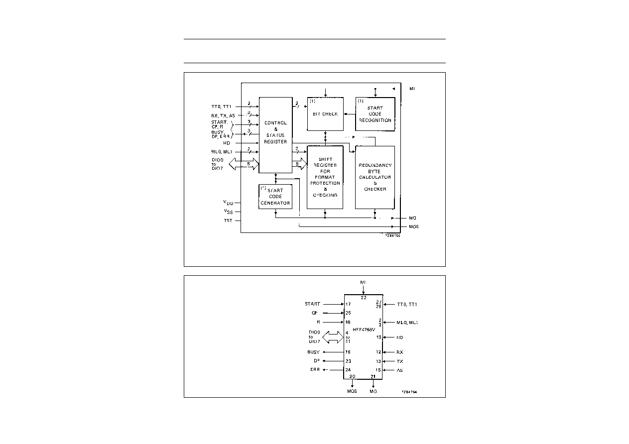
Fig.2 Block diagram.
(1) Only used in the asynchronous mode.
Fig.3 Functional diagram.
January 1995
6
Philips Semiconductors
Product specification
Transceiver for serial data communication
HEF4755V
LSI
FUNCTIONAL DESCRIPTION
General
The HEF4755V is used for protected-bit serial data
communication. This protection makes it necessary to
subdivide the serial data stream into data blocks called
messages.
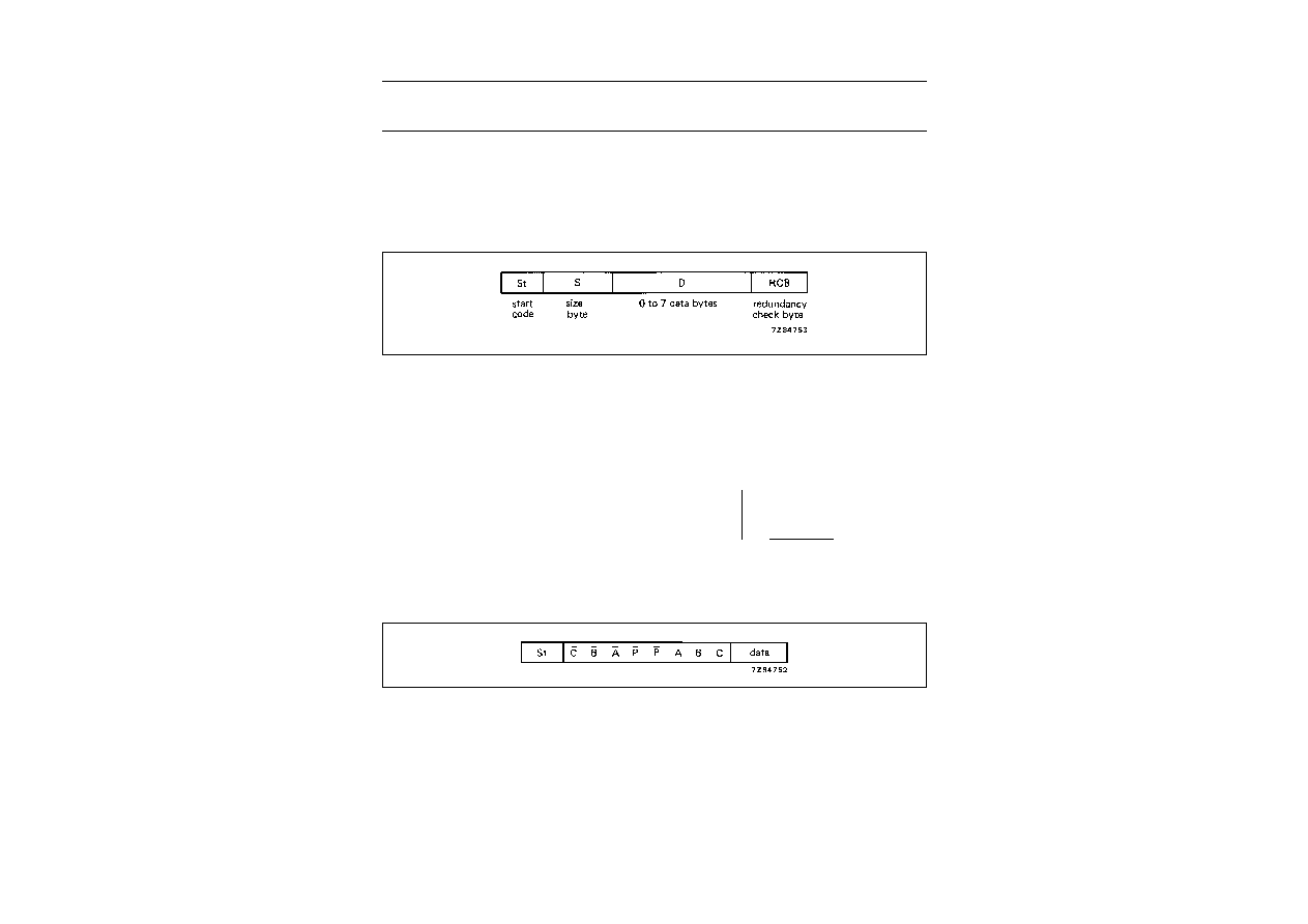
Messages
In the synchronous mode the HEF4755V will transmit or
receive a message as follows:
The first bit of a transmitted message is the start-bit which
cannot be mis interpreted. It instructs the receiver, that
information transfer has started and it defines the
time-window for the following bits. The start-bit is only
necessary in the asynchronous mode and it is omitted in
the synchronous mode. The first byte contains the number
of data bytes that will follow. This byte is checked by the
receiver and if a discrepancy is found, the receiver reports
a code-error. This first byte is called `size'. The number of
data bytes can also be fixed by wiring of the transmitter as
well as the receiver. In this case the size byte is omitted.
There is no protocol on the information of the data bytes,
so the maximum number of informations per message is
2
56
10
17
.
The redundancy check byte secures the data bytes
against transmission errors. This byte is calculated in
parallel to the data stream and it is send as last byte by the
transmitter. The receiver calculates its own redundancy
byte and compares it with the received one. If there is a
discrepancy, the receiver reports a code error.
Code protection
Size
The coding of the size byte is as follows:
DIO0 = C
DIO1 = B
n = C
2
2
+
B
2
1
+
A
2
0
DIO2 = A
DIO3 = P
= C
B
A
The information is transmitted as follows:
With this, a hamming distance of 4 is obtained.

January 1995
7
Philips Semiconductors
Product specification
Transceiver for serial data communication
HEF4755V
LSI
Redundancy byte
The redundancy byte completes the data bytes with 15 (7)
bits as a code word. If only one bit in the information has
changed during the transmission, the two code words will
differ by at least 6 (4) bit positions. So a change of up to 5
(3) bits will always be observed, even every odd number of
false bits will be recognized. The HEF4755V has a
programmable redundancy bit calculator which carries out
this protection (the numbers given in parentheses are valid
for the alternative possibility).
If the transmission line carries extreme noise, this kind of
message protection is less effective. In this case, the
message is protected by checking bit-per-bit in a smaller
time scale (see `bit protection' below).
Bit protection
The HEF4755V checks every received bit within the time
window defined by the start-bit. The programmed time
tolerance (19%, 25%, 31% and 37%) determines that the
bit protection circuit decides after 32 samples which bit is
a true logic HIGH or LOW level, or an error. In the latter
case, there are too many samples HIGH to obtain a LOW
and, too many samples LOW to obtain a HIGH.
Transmitting
In the transmitting mode the HEF4755V uses the data
pulse signal (DP, pin 23) to take 8 bits from the data bus.
These parallel bits are shifted serially to the message
output (MO).
Receiving
In the receiving mode the HEF4755V receives serial bits at
the message input (MI). The circuit checks the message
for transmission errors and, with every data pulse, 8 bits
are transferred in parallel to the data bus. Every
recognized error is stored and the error output is activated.
The kind of error can be recognized by reading the status
register over the data bus.
Asynchronous and synchronous mode
If only one transmission line is available, then the receiver
waits for the start-bit, synchronizes itself on the start bit
and receives all the data bits of one message. This is
called the
asynchronous mode. By using 3 transmission
lines, the circuit can go to the
synchronous mode. In this
case it is possible to transmit also the clock signal (CP)
and message synchronization signal (MOS) in parallel with
the data bits. The start bit and the bit check are omitted. In
the synchronous mode the maximum transmission speed
is 32 times the maximum speed in the asynchronous
mode.
In asynchronous receive mode a reset pulse is necessary
between two messages. It is possible to derive this reset
pulse from the busy signal by using hardware. The
duration of the START-pulse at the transmitter must
always be shorter than the message to be transferred. A
good procedure for achieving this is to use the
BUSY-signal to end the START-pulse. The recovery time
between two messages must be at least two bit periods.
During this time, the line must remain stable to prevent
generation of an error. This must be ensured with external
hardware/software.
In the synchronous receive mode, the duration of the
START-pulse at the transmitter must always be shorter
than the message to be transferred. A good procedure for
achieving this is to use the BUSY-signal to end the
START-pulse. A continuous START-signal will cause
malfunction. The recovery time between two messages
must be at least one bit period. During this time, the
message line must remain stable. A good way to achieve
this is to use the trailing-edge of the BUSY-signal to
generate a START-signal. In practice, if data is delivered
to the transmitter fast enough, START can be BUSY. If the
lines have different delays, the message line should have
the longest delay. If it is not certain which line has the
longest delay it is possible to phase-shift the clock signal
of the receiver by inverting it. This is only possible with
point-to-point lines.

January 1995
8
Philips Semiconductors
Product specification
Transceiver for serial data communication
HEF4755V
LSI
DC CHARACTERISTICS
V
SS
= 0 V; T
amb
=
-
40 to
+
85
°
C; unless otherwise specified
PARAMETER
V
DD
V
SYMBOL
MIN.
TYP.
MAX.
UNIT
CONDITIONS
Outputs
Output voltage LOW
4,75 to
12,6
V
OL
-
-
0,4 V
I
OL
= 1,8 mA
4,75
V
OL
-
-
0,4 V
I
OL
= 2,3 mA
T
amb
= 25
°
C
Output voltage HIGH
4,75 to
12,6
V
OH
V
DD
-
1
-
-
V
-
I
OH
= 1,1 mA
4,75
V
OH
V
DD
-
1
-
-
V
-
I
OH
= 1,4 mA
T
amb
= 25
°
C
Inputs/outputs
As outputs
Output voltage LOW
4,75 to
12,6
V
OL
-
-
0,4 V
I
OL
= 1,8 mA
4,75
V
OL
-
-
0,4 V
I
OL
= 2,3 mA
T
amb
= 25
°
C
Output voltage HIGH
4,75 to
12,6
V
OH
V
DD
-
1
-
-
V
-
I
OH
= 1,1 mA
4,75
V
OH
V
DD
-
1
-
-
V
-
I
OH
= 1,4 mA
T
amb
= 25
°
C
Output leakage current
HIGH
12,6
I
OZH
-
-
20
µ
A
V
OH
= 12,6 V
12,6
I
OZH
-
-
5
µ
A
V
OH
= 12,6 V
T
amb
= 25
°
C
LOW
-
I
OZL
-
-
20
µ
A
V
OL
= 0 V
-
I
OZL
-
-
5
µ
A
V
OL
= 0 V
T
amb
= 25
°
C
As inputs
Input voltage LOW
4,75 to
12,6
V
IL
0
-
0,3 V
DD
V
Input voltage HIGH
4,75 to
12,6
V
IH
0,7 V
DD
-
V
DD
V

January 1995
9
Philips Semiconductors
Product specification
Transceiver for serial data communication
HEF4755V
LSI
AC CHARACTERISTICS
V
SS
= 0 V; T
amb
=
-
40 to
+
85
°
C; unless otherwise specified
Note
1. Measured between output voltage levels of 0,8 V and 2 V.
PARAMETER
V
DD
V
SYMBOL
MIN.
TYP.
MAX.
UNIT
CONDITIONS
Asynchronous mode
AS at V
DD
Clock pulse width
LOW
5
t
WCPL
500
ns
10
125
ns
HIGH
5
t
WCPH
500
ns
10
125
ns
START pulse
5
t
WSH
0,9
µ
s
width HIGH
10
0,22
µ
s
Set-up time
5
t
su
1,4
µ
s
D
n
CP
10
0,35
µ
s
Hold time
5
t
hold
0
µ
s
CP
D
n
10
0
µ
s
Reset (R) pulse
5
t
WRH
1
µ
s
width HIGH
10
0,25
µ
s
Synchronous mode
AS at V
SS
Clock pulse width
5
t
WCPL
625
ns
LOW
10
150
ns
HIGH
5
t
WCPH
625
ns
10
150
ns
Set-up time
5
t
su
0,6
µ
s
START
CP
10
0,15
µ
s
Hold time
5
t
hold
300
ns
CP
START
10
75
ns
Set-up time
5
t
su
600
ns
D
n
CP
10
150
ns
Hold time
5
t
hold
0
ns
CP
D
n
10
0
ns
Reset (R) pulse
5
t
WRH
1
µ
s
width HIGH
10
0,25
µ
s
January 1995
10
Philips Semiconductors
Product specification
Transceiver for serial data communication
HEF4755V
LSI
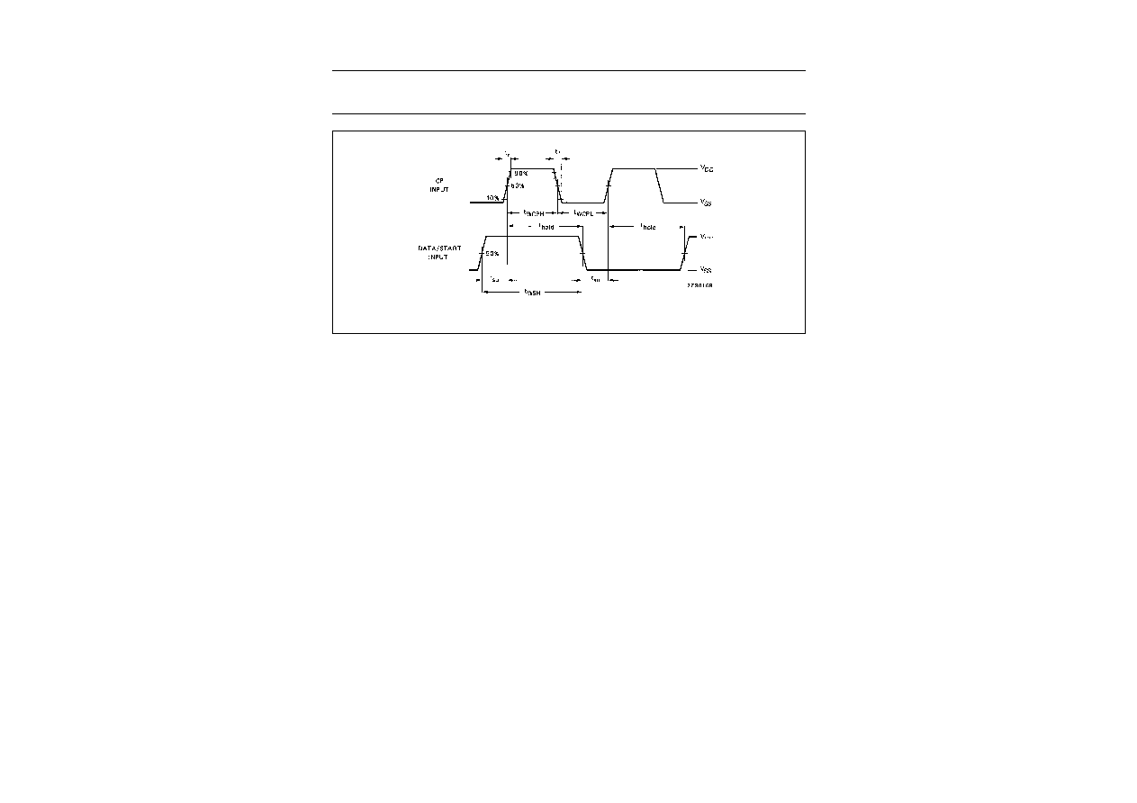
Fig.6 Waveforms showing the clock, data and start timing.

January 1995
11
Philips Semiconductors
Product specification
T
ransceiver for serial data communication
HEF4755V
LSI
This text is here in white to force landscape pages to be rotated correctly when browsing through the pdf in the Acrobat reader.This text is here in
_
white to force landscape pages to be rotated correctly when browsing through the pdf in the Acrobat reader.This text is here inThis text is here in
white to force landscape pages to be rotated correctly when browsing through the pdf in the Acrobat reader. white to force landscape pages to be ...
Fig.7
Function/timing diagram when using the HEF4755V in the asynchronous mode where the byte number per message is variable and the
hamming distance is 4.

January 1995
12
Philips Semiconductors
Product specification
T
ransceiver for serial data communication
HEF4755V
LSI
This text is here in white to force landscape pages to be rotated correctly when browsing through the pdf in the Acrobat reader.This text is here in
_
white to force landscape pages to be rotated correctly when browsing through the pdf in the Acrobat reader.This text is here inThis text is here in
white to force landscape pages to be rotated correctly when browsing through the pdf in the Acrobat reader. white to force landscape pages to be ...
Fig.8
Function/timing diagram when using the HEF4755V in the asynchronous mode where the byte number per message is variable and the
hamming distance is 4.
Document Outline
- DESCRIPTION
- FEATURES
- SUPPLY VOLTAGE/CURRENT
- FAMILY DATA, IDD LIMITS category LSI
- PINNING
- FUNCTIONAL DESCRIPTION
- General
- Messages
- Code protection
- Bit protection
- Transmitting
- Receiving
- Asynchronous and synchronous mode
- DC CHARACTERISTICS
- AC CHARACTERISTICS