 | –≠–ª–µ–∫—Ç—Ä–æ–Ω–Ω—ã–π –∫–æ–º–ø–æ–Ω–µ–Ω—Ç: J109 | –°–∫–∞—á–∞—Ç—å:  PDF PDF  ZIP ZIP |
DATA SHEET
Product specification
Supersedes data of April 1995
File under Discrete Semiconductors, SC07
1996 Jul 30
DISCRETE SEMICONDUCTORS
J108; J109; J110
N-channel silicon junction FETs
1996 Jul 30
2
Philips Semiconductors
Product specification
N-channel silicon junction FETs
J108; J109; J110
FEATURES
∑
High speed switching
∑
Interchangeability of drain and source connections
∑
Low R
DSon
at zero gate voltage (<8
for J108).
APPLICATIONS
∑
Analog switches
∑
Choppers and commutators.
DESCRIPTION
N-channel symmetrical silicon junction field-effect
transistors in a TO-92 package.
CAUTION
The device is supplied in an antistatic package. The
gate-source input must be protected against static
discharge during transport or handling.
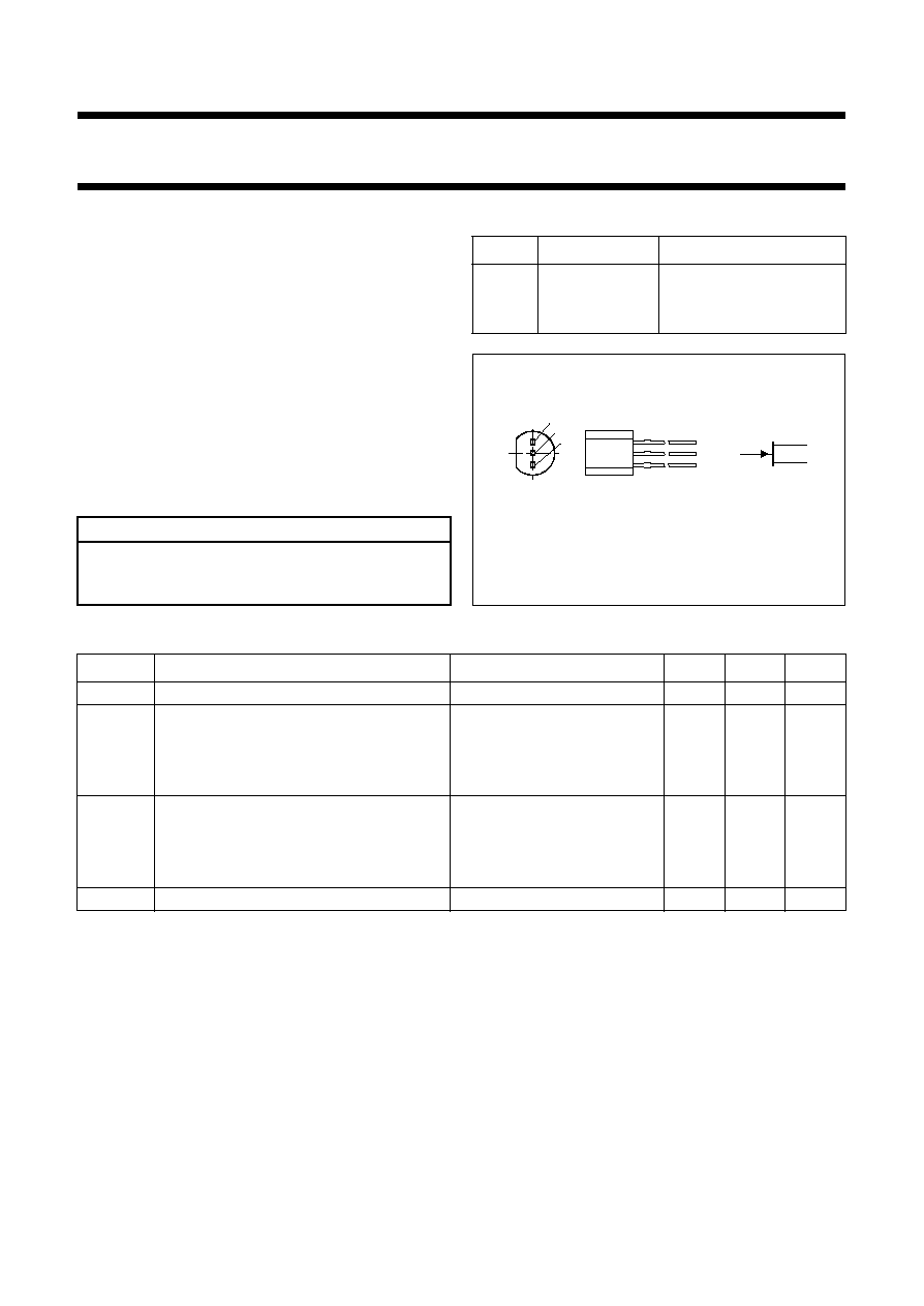
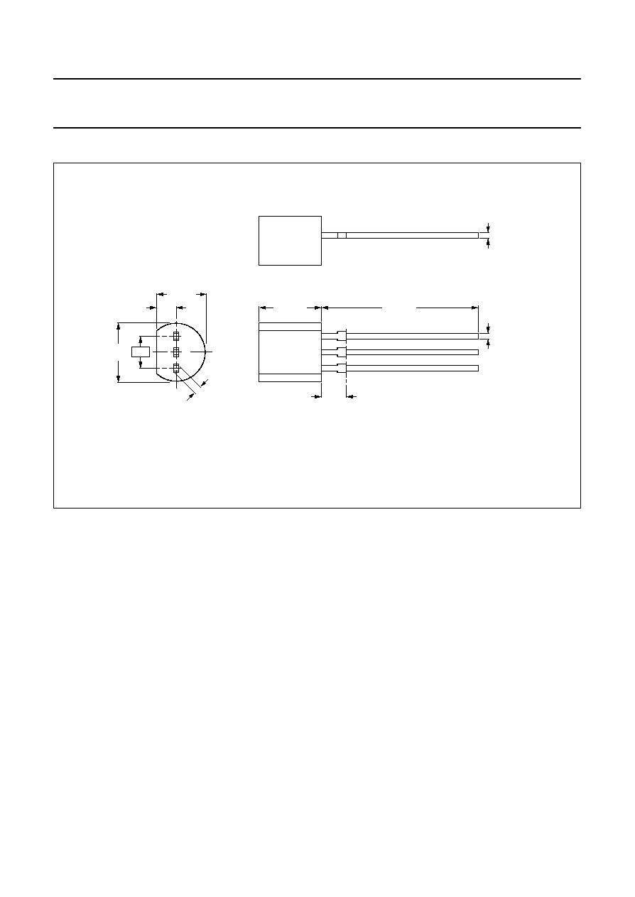
PINNING - TO-92
PIN
SYMBOL
DESCRIPTION
1
g
gate
2
s
source
3
d
drain
Fig.1 Simplified outline and symbol.
handbook, halfpage
1
3
2
MAM197
s
d
g
QUICK REFERENCE DATA
SYMBOL
PARAMETER
CONDITIONS
MIN.
MAX.
UNIT
V
DS
drain-source voltage
-
±
25
V
V
GSoff
gate-source cut-off voltage
I
D
= 1
µ
A; V
DS
= 5 V
J108
-
3
-
10
V
J109
-
2
-
6
V
J110
-
0.5
-
4
V
I
DSS
drain current
V
GS
= 0; V
DS
= 5 V
J108
80
-
mA
J109
40
-
mA
J110
10
-
mA
P
tot
total power dissipation
up to T
amb
= 50
∞
C
-
400
mW
1996 Jul 30
3
Philips Semiconductors
Product specification
N-channel silicon junction FETs
J108; J109; J110
LIMITING VALUES
In accordance with the Absolute Maximum Rating System (IEC 134).
THERMAL CHARACTERISTICS
STATIC CHARACTERISTICS
T
j
= 25
∞
C; unless otherwise specified.
SYMBOL
PARAMETER
CONDITIONS
MIN.
MAX.
UNIT
V
DS
drain-source voltage
-
±
25
V
V
GSO
gate-source voltage
open drain
-
-
25
V
V
GDO
gate-drain voltage
open source
-
-
25
V
I
G
forward gate current (DC)
-
50
mA
P
tot
total power dissipation
up to T
amb
= 50
∞
C
-
400
mW
T
stg
storage temperature
-
65
150
∞
C
T
j
operating junction temperature
-
150
∞
C
SYMBOL
PARAMETER
VALUE
UNIT
R
th j-a
thermal resistance from junction to ambient
250
K/W
SYMBOL
PARAMETER
CONDITIONS
MIN.
TYP.
MAX.
UNIT
V
(BR)GSS
gate-source breakdown voltage
I
G
=
-
1
µ
A; V
DS
= 0
-
-
-
25
V
V
GSoff
gate-source cut-off voltage
I
D
= 1
µ
A; V
DS
= 5 V
V
J108
-
3
-
-
10
V
J109
-
2
-
-
6
V
J110
-
0.5
-
-
4
V
I
DSS
drain current
V
GS
= 0; V
DS
= 15 V
J108
80
-
-
mA
J109
40
-
-
mA
J110
10
-
-
mA
I
GSS
gate leakage current
V
GS
=
-
15 V; V
DS
= 0
-
-
-
3
nA
I
DSX
drain-source cut-off current
V
GS
=
-
10 V; V
DS
= 5 V
-
-
3
nA
R
DSon
drain-source on-state resistance
V
GS
= 0; V
DS
= 100 mV
J108
-
-
8
J109
-
-
12
J110
-
-
18
1996 Jul 30
4
Philips Semiconductors
Product specification
N-channel silicon junction FETs
J108; J109; J110
DYNAMIC CHARACTERISTICS
T
j
= 25
∞
C; unless otherwise specified.
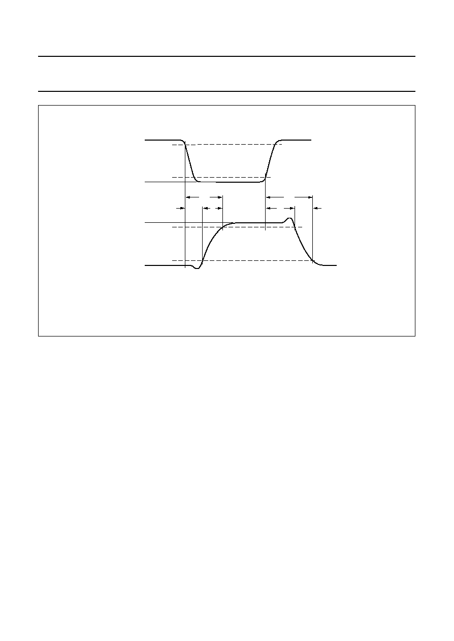
Note
1. Test conditions for switching times are as follows:
V
DD
= 1.5 V; V
GS
= 0 to V
GSoff
(all types)
V
GSoff
=
-
12 V; R
L
= 100
(J108)
V
GSoff
=
-
7 V; R
L
= 100
(J109)
V
GSoff
=
-
5 V; R
L
= 100
(J110).
SYMBOL
PARAMETER
CONDITIONS
TYP.
MAX.
UNIT
C
is
input capacitance
V
DS
= 0; V
GS
=
-
10 V; f = 1 MHz
15
30
pF
V
DS
= 0; V
GS
= 0; f = 1 MHz;
T
amb
= 25
∞
C
50
85
pF
C
rs
reverse transfer capacitance
V
DS
= 0; V
GS
=
-
10 V; f = 1 MHz
8
15
pF
Switching times; see Fig.2
t
d
delay time
note 1
2
-
ns
t
on
turn-on time
4
-
ns
t
s
storage time
4
-
ns
t
off
turn-off time
6
-
ns
Fig.2 Switching circuit.
handbook, halfpage
MGE773
RL
50
DUT
SAMPLING
SCOPE
50
50
0.1
µ
F
10
µ
F
10 nF
VDD
1996 Jul 30
5
Philips Semiconductors
Product specification
N-channel silicon junction FETs
J108; J109; J110
Fig.3 Input and output waveforms.
handbook, full pagewidth
MGE774
VGS off
toff
tf
ts
VGS = 0 V
Vi
Vo
10%
90%
90%
10%
ton
td
tr
1996 Jul 30
6
Philips Semiconductors
Product specification
N-channel silicon junction FETs
J108; J109; J110
PACKAGE OUTLINE
Fig.4 TO-92 (SOT54).
Dimensions in mm.
(1) Terminal dimensions in this zone are uncontrolled.
andbook, full pagewidth
MBC014 - 1
2.54
4.8
max
4.2 max
1.7
1.4
0.66
0.56
1
2
3
5.2 max
12.7 min
2.0 max
(1)
0.48
0.40
0.40
min
1996 Jul 30
7
Philips Semiconductors
Product specification
N-channel silicon junction FETs
J108; J109; J110
DEFINITIONS
LIFE SUPPORT APPLICATIONS
These products are not designed for use in life support appliances, devices, or systems where malfunction of these
products can reasonably be expected to result in personal injury. Philips customers using or selling these products for
use in such applications do so at their own risk and agree to fully indemnify Philips for any damages resulting from such
improper use or sale.
Data Sheet Status
Objective specification
This data sheet contains target or goal specifications for product development.
Preliminary specification
This data sheet contains preliminary data; supplementary data may be published later.
Product specification
This data sheet contains final product specifications.
Limiting values
Limiting values given are in accordance with the Absolute Maximum Rating System (IEC 134). Stress above one or
more of the limiting values may cause permanent damage to the device. These are stress ratings only and operation
of the device at these or at any other conditions above those given in the Characteristics sections of the specification
is not implied. Exposure to limiting values for extended periods may affect device reliability.
Application information
Where application information is given, it is advisory and does not form part of the specification.