DATA SHEET
Product specification
File under Discrete Semiconductors, SC07
April 1995
DISCRETE SEMICONDUCTORS
J174; J175;
J176; J177
P-channel silicon field-effect
transistors
April 1995
2
Philips Semiconductors
Product specification
P-channel silicon field-effect transistors
J174; J175;
J176; J177
DESCRIPTION
Silicon symmetrical p-channel
junction FETs in a plastic TO-92
envelope and intended for application
with analog switches, choppers,
commutators etc.
A special feature is the
interchangeability of the drain and
source connections.
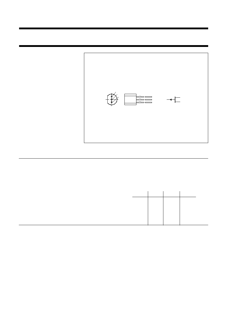
PINNING
Note: Drain and source are
interchangeable.
1 =
source
2 =
gate
3 =
drain
Fig.1 Simplified outline and symbol, TO-92.
handbook, halfpage
1
3
2
MAM388
s
d
g
QUICK REFERENCE DATA
Drain-source voltage
�
V
DS
max.
30
V
Gate-source voltage
V
GSO
max.
30
V
Gate current
-
I
G
max.
50
mA
Total power dissipation
up to T
amb
= 50
�
C
P
tot
max.
400
mW
J174
J175
J176
J177
Drain current
min.
max.
20
135
7
70
2
35
1.5
20
mA
mA
-
V
DS
= 15 V; V
GS
= 0
-
I
DSS
Drain-source ON-resistance
-
V
DS
= 0.1 V; V
GS
= 0
R
DS on
max.
85
125
250
300
April 1995
3
Philips Semiconductors
Product specification
P-channel silicon field-effect transistors
J174; J175;
J176; J177
RATINGS
Limiting values in accordance with the Absolute Maximum System (IEC 134)
THERMAL RESISTANCE
STATIC CHARACTERISTICS
Drain-source voltage
�
V
DS
max.
30
V
Gate-source voltage
V
GSO
max.
30
V
Gate-drain voltage
V
GDO
max.
30
V
Gate current (DC)
-
I
G
max.
50
mA
Total power dissipation
up to T
amb
= 50
�
C
P
tot
max.
400
mW
Storage temperature range
T
stg
-
65 to
+
150
�
C
Junction temperature
T
j
max.
150
�
C
From junction to ambient in free air
R
th j-a
=
250
K/W
T
j
= 25
�
C unless otherwise specified
J174
J175
J176 J177
Gate cut-off current
V
GS
= 20 V; V
DS
= 0
I
GSS
max.
1
1
1
1 nA
Drain cut-off current
-
V
DS
= 15 V; V
GS
= 10 V
-
I
DSX
max.
1
1
1
1 nA
Drain current
-
V
DS
= 15 V; V
GS
= 10 V
-
I
DSS
min.
20
7
2
1.5 mA
max.
135
70
35
20 mA
Gate-source breakdown voltage
I
G
= 1
�
A; V
DS
= 0
V
(BR)GSS
min.
30
30
30
30 V
Gate-source cut-off voltage
-
I
D
= 10 nA; V
DS
=
-
15 V
V
GS off
min.
5
3
1
0.8 V
max.
10
6
4
2.25 V
Drain-source ON-resistance
-
V
DS
= 0.1 V; V
GS
= 0
R
DSon
max.
85
125
250
300
April 1995
4
Philips Semiconductors
Product specification
P-channel silicon field-effect transistors
J174; J175;
J176; J177
DYNAMIC CHARACTERISTICS
T
j
= 25
�
C unless otherwise specified
Input capacitance, f = 1 MHz
V
GS
= 10 V; V
DS
= 0 V
C
is
typ.
8
pF
V
GS
= V
DS
= 0
C
is
typ.
30
pF
Feedback capacitance, f = 1 MHz
V
GS
= 10 V; V
DS
= 0 V
C
rs
typ.
4
pF
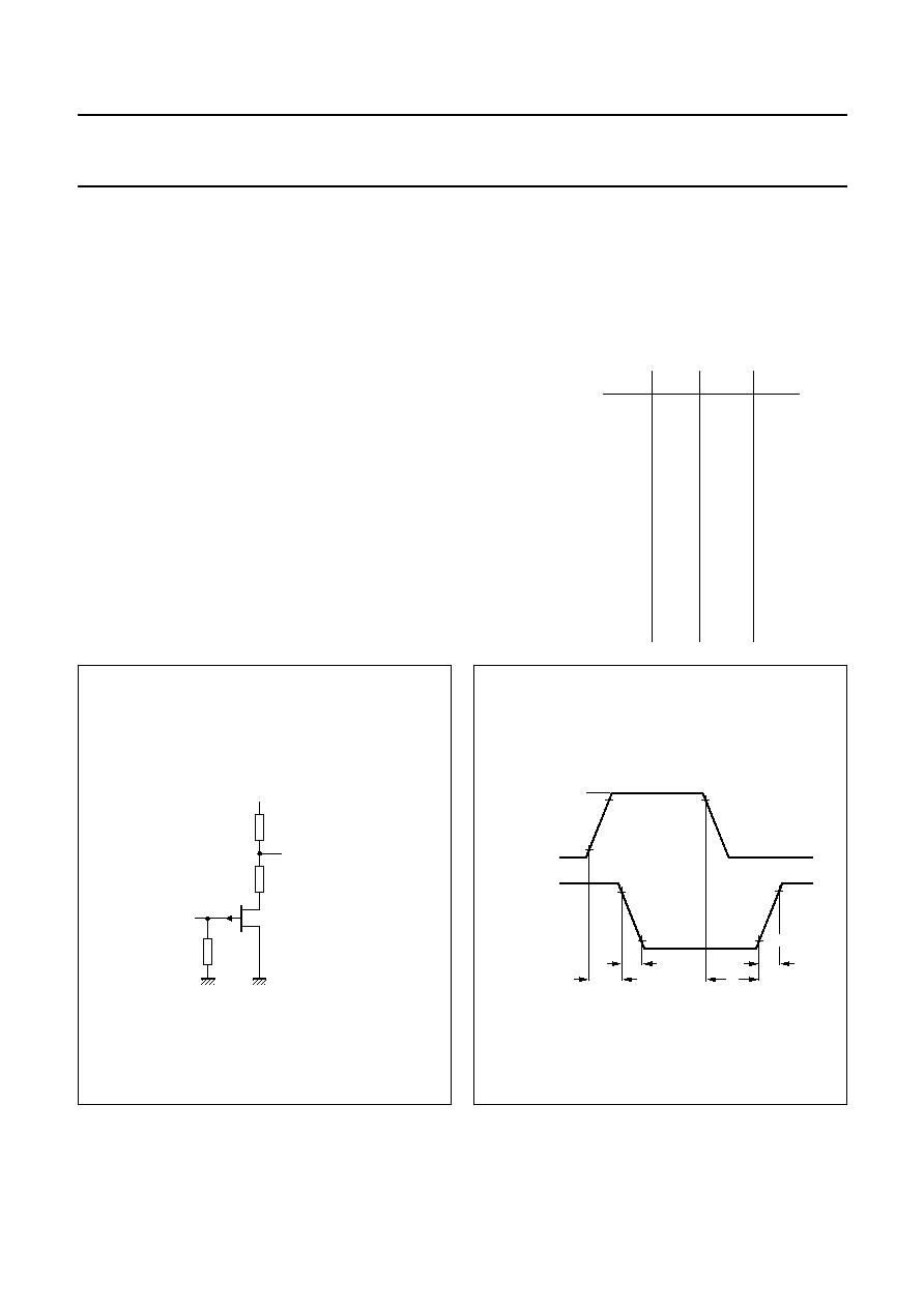
Switching times (see Fig.2
+
3)
J174
J175
J176 J177
Delay time
t
d
typ.
2
5
15
20 ns
Rise time
t
r
typ.
5
10
20
25 ns
Turn-on time
t
on
typ.
7
15
35
45 ns
Storage time
t
s
typ.
5
10
15
20 ns
Fall time
t
f
typ.
10
20
20
25 ns
Turn-off time
t
off
typ.
15
30
35
45 ns
Test conditions:
-
V
DD
10
6
6
6 V
V
GS off
12
8
6
3 V
R
L
560
1200
2000 2900
V
GS on
0
0
0
0 V
Fig.2 Switching times test circuit.
handbook, halfpage
MBK292
RL
50
D.U.T
50
Vin
Vout
-
VDD
Fig.3 Input and output waveforms;
t
d
+
t
r
= t
on
; t
s
+ t
f
= t
off
.
MBK293
VGSoff
INPUT
OUTPUT
ts
tf
90%
10%
10%
90%
10%
90%
td
tr
April 1995
5
Philips Semiconductors
Product specification
P-channel silicon field-effect transistors
J174; J175;
J176; J177
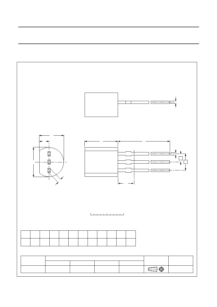
PACKAGE OUTLINE
UNIT
A
REFERENCES
OUTLINE
VERSION
EUROPEAN
PROJECTION
ISSUE DATE
IEC
JEDEC
EIAJ
mm
5.2
5.0
b
0.48
0.40
c
0.45
0.40
D
4.8
4.4
d
1.7
1.4
E
4.2
3.6
L
14.5
12.7
e
2.54
e1
1.27
L1
(1)
2.5
b1
0.66
0.56
DIMENSIONS (mm are the original dimensions)
Note
1. Terminal dimensions within this zone are uncontrolled to allow for flow of plastic and terminal irregularities.
SOT54
TO-92
SC-43
97-02-28
A
L
0
2.5
5 mm
scale
b
c
D
b
1
L1
d
E
Plastic single-ended leaded (through hole) package; 3 leads
SOT54
e1
e
1
2
3
April 1995
6
Philips Semiconductors
Product specification
P-channel silicon field-effect transistors
J174; J175;
J176; J177
DEFINITIONS
LIFE SUPPORT APPLICATIONS
These products are not designed for use in life support appliances, devices, or systems where malfunction of these
products can reasonably be expected to result in personal injury. Philips customers using or selling these products for
use in such applications do so at their own risk and agree to fully indemnify Philips for any damages resulting from such
improper use or sale.
Data sheet status
Objective specification
This data sheet contains target or goal specifications for product development.
Preliminary specification
This data sheet contains preliminary data; supplementary data may be published later.
Product specification
This data sheet contains final product specifications.
Short-form specification
The data in this specification is extracted from a full data sheet with the same type
number and title. For detailed information see the relevant data sheet or data handbook.
Limiting values
Limiting values given are in accordance with the Absolute Maximum Rating System (IEC 134). Stress above one or
more of the limiting values may cause permanent damage to the device. These are stress ratings only and operation
of the device at these or at any other conditions above those given in the Characteristics sections of the specification
is not implied. Exposure to limiting values for extended periods may affect device reliability.
Application information
Where application information is given, it is advisory and does not form part of the specification.