 | ÐлекÑÑоннÑй компоненÑ: LM124/BCA | СкаÑаÑÑ:  PDF PDF  ZIP ZIP |
LM124/224/324/324A/SA534/LM2902 Low power quad op amps
Philips
Semiconductors
Product data
Supersedes data of 2002 Jul 12
LM124/224/324/324A/
SA534/LM2902
Low power quad op amps
2003 Sep 19
INTEGRATED CIRCUITS
Philips Semiconductors
Product data
LM124/224/324/324A/
SA534/LM2902
Low power quad op amps
2
2003 Sep 19
DESCRIPTION
The LM124/SA534/LM2902 series consists of four independent,
high-gain, internally frequency-compensated operational amplifiers
designed specifically to operate from a single power supply over a
wide range of voltages.
UNIQUE FEATURES
In the linear mode, the input common-mode voltage range includes
ground and the output voltage can also swing to ground, even
though operated from only a single power supply voltage.
The unity gain crossover frequency and the input bias current are
temperature-compensated.
FEATURES
·
Internally frequency-compensated for unity gain
·
Large DC voltage gain: 100 dB
·
Wide bandwidth (unity gain): 1 MHz (temperature-compensated)
·
Wide power supply range Single supply: 3 V
DC
to 30 V
DC
or dual
supplies:
±
1.5 V
DC
to
±
15 V
DC
·
Very low supply current drain: essentially independent of supply
voltage (1 mW/op amp at +5 V
DC
)
·
Low input biasing current: 45 nA
DC
(temperature-compensated)
·
Low input offset voltage: 2 mV
DC
and offset current: 5 nA
DC
·
Differential input voltage range equal to the power supply voltage
·
Large output voltage: 0V
DC
to V
CC
1.5 V
DC
swing
PIN CONFIGURATION
D, DH, and N Packages
1
2
3
4
5
6
7
8
14
13
12
11
10
9
+
1
+
4
+
2
+
3
OUTPUT 1
INPUT 1
+INPUT 1
V +
+INPUT 2
INPUT 2
OUTPUT 2
OUTPUT 4
INPUT 4
+INPUT 4
GND
+INPUT 3
INPUT 3
OUTPUT 3
TOP VIEW
SL00065
Figure 1. Pin configuration.
ORDERING INFORMATION
DESCRIPTION
TEMPERATURE RANGE
ORDER CODE
DWG #
14-Pin Plastic Dual In-Line Package (DIP)
55
°
C to +125
°
C
LM124N
SOT27-1
14-Pin Plastic Small Outline (SO) Package
25
°
C to +85
°
C
LM224D
SOT108-1
14-Pin Plastic Dual In-Line Package (DIP)
25
°
C to +85
°
C
LM224N
SOT27-1
14-Pin Plastic Small Outline (SO) Package
0
°
C to +70
°
C
LM324AD
SOT108-1
14-Pin Plastic Dual In-Line Package (DIP)
0
°
C to +70
°
C
LM324AN
SOT27-1
14-Pin Plastic Small Outline (SO) Package
0
°
C to +70
°
C
LM324D
SOT108-1
14-Pin Plastic Thin Shrink Small Outline Package (TSSOP)
0
°
C to +70
°
C
LM324DH
SOT402-1
14-Pin Plastic Dual In-Line Package (DIP)
0
°
C to +70
°
C
LM324N
SOT27-1
14-Pin Plastic Small Outline (SO) Package
40
°
C to +85
°
C
SA534D
SOT108-1
14-Pin Plastic Dual In-Line Package (DIP)
40
°
C to +85
°
C
SA534N
SOT27-1
14-Pin Plastic Small Outline (SO) Package
40
°
C to +125
°
C
LM2902D
SOT108-1
14-Pin Plastic Thin Shrink Small Outline Package (TSSOP)
40
°
C to +125
°
C
LM2902DH
SOT402-1
14-Pin Plastic Dual In-Line Package (DIP)
40
°
C to +125
°
C
LM2902N
SOT27-1
Philips Semiconductors
Product data
LM124/224/324/324A/
SA534/LM2902
Low power quad op amps
2003 Sep 19
3
ABSOLUTE MAXIMUM RATINGS
SYMBOL
PARAMETER
RATING
UNIT
V
CC
Supply voltage
32 or
±
16
V
DC
V
IN
Differential input voltage
32
V
DC
V
IN
Input voltage
0.3 to +32
V
DC
P
D
Maximum power dissipation, T
amb
= 25
°
C (still-air)
1
N package
1420
mW
D package
1040
mW
DH package
762
mW
Output short-circuit to GND one amplifier
2
Continuous
V
CC
< 15 V
DC
and T
amb
= 25
°
C
Continuous
I
IN
Input current (V
IN
< 0.3 V)
3
50
mA
T
amb
Operating ambient temperature range
LM324/324A
0 to +70
°
C
LM224
25 to +85
°
C
SA534
40 to +85
°
C
LM2902
40 to +125
°
C
LM124
55 to +125
°
C
T
stg
Storage temperature range
65 to +150
°
C
T
sld
Lead soldering temperature (10 sec max)
230
°
C
NOTES:
1. Derate above 25
°
C
at the following rates:
N package at 11.4 mW/
°
C
D package at 8.3 mW/
°
C
DH package at 6.1mW/
°
C
2. Short-circuits from the output to V
CC
+ can cause excessive heating and eventual destruction. The maximum output current is approximately
40 mA, independent of the magnitude of V
CC
. At values of supply voltage in excess of +15 V
DC
continuous short-circuits can exceed the
power dissipation ratings and cause eventual destruction.
3. This input current will only exist when the voltage at any of the input leads is driven negative. It is due to the collector-base junction of the
input PNP transistors becoming forward biased and thereby acting as input bias clamps. In addition, there is also lateral NPN parasitic
transistor action on the IC chip. This action can cause the output voltages of the op amps to go to the V+ rail (or to ground for a large
overdrive) during the time that the input is driven negative.
Philips Semiconductors
Product data
LM124/224/324/324A/
SA534/LM2902
Low power quad op amps
2003 Sep 19
4
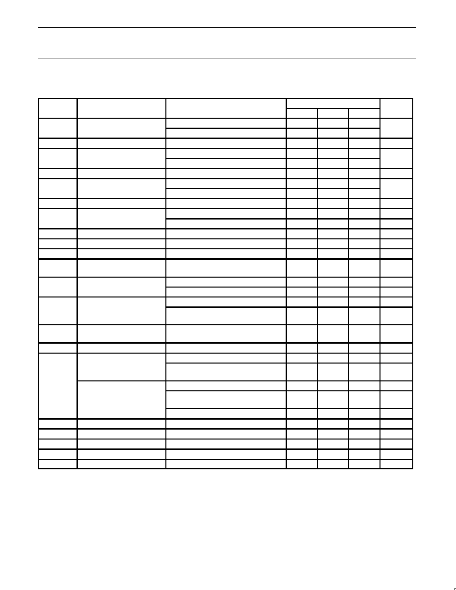
DC ELECTRICAL CHARACTERISTICS
V
CC
= 5 V; T
amb
= 25
°
C, unless otherwise specified.
SYMBOL
PARAMETER
TEST CONDITIONS
LM124/LM224
LM324/SA534/LM2902
UNIT
SYMBOL
PARAMETER
TEST CONDITIONS
Min
Typ
Max
Min
Typ
Max
UNIT
V
OS
Offset voltage
1
R
S
= 0
±
2
±
5
±
2
±
7
mV
V
OS
Offset voltage
1
R
S
= 0
, over temp.
±
7
±
9
mV
V
OS
/
T
Temperature drift
R
S
= 0
, over temp.
7
7
µ
V/
°
C
I
S
Input current
2
I
IN
(+) or I
IN
()
45
150
45
250
nA
I
BIAS
Input current
2
I
IN
(+) or I
IN
(), over temp.
40
300
40
500
nA
I
BIAS
/
T
Temperature drift
Over temp.
50
50
pA/
°
C
I
OS
Offset current
I
IN
(+)I
IN
()
±
3
±
30
±
5
±
50
nA
I
OS
Offset current
I
IN
(+)I
IN
(), over temp.
±
100
±
150
nA
I
OS
/
T
Temperature drift
Over temp.
10
10
pA/
°
C
V
C
Common-mode voltage
V
CC
30 V
0
V
CC
1.5
0
V
CC
1.5
V
V
CM
g
range
3
V
CC
30 V; over temp.
0
V
CC
2
0
V
CC
2
V
CMRR
Common-mode rejection
ratio
V
CC
= 30 V
70
85
65
70
dB
V
OUT
Output voltage swing
R
L
= 2 k
, V
CC
= 30 V,
over temp.
26
26
V
V
OH
Output voltage high
R
L
10 k
, V
CC
= 30 V,
over temp.
27
28
27
28
V
V
OL
Output voltage low
R
L
10 k
; over temp.
5
20
5
20
mV
I
CC
Supply current
R
L
=
, V
CC
= 30 V; over temp.
1.5
3
1.5
3
mA
I
CC
Supply current
R
L
=
; over temp.
0.7
1.2
0.7
1.2
mA
A
O
Large signal voltage gain
V
CC
= 15 V (for large V
O
swing);
R
L
2 k
50
100
25
100
V/mV
A
VOL
Large-signal voltage gain
V
CC
= 15 V (for large V
O
swing);
R
L
2k
; over temp.
25
15
V/mV
Amplifier-to-amplifier
coupling
5
f = 1 kHz to 20 kHz,
input referred
120
120
dB
PSRR
Power supply rejection ratio
R
S
0
65
100
65
100
dB
Output current source
V
IN
+ = +1 V, V
IN
= 0 V,
V
CC
= 15 V
20
40
20
40
Output current source
V
IN
+ = +1 V, V
IN
= 0 V,
V
CC
= 15 V, over temp.
10
20
10
20
mA
I
OUT
V
IN
= +1 V, V
IN
+ = 0 V,
V
CC
= 15 V
10
20
10
20
mA
Output current sink
V
IN
= +1 V, V
IN
+ = 0 V,
V
CC
= 15 V, over temp.
5
8
5
8
V
IN
= +1 V, V
IN
+ = 0 V,
V
O
= 200 mV
12
50
12
50
µ
A
I
SC
Short-circuit current
4
10
40
60
10
40
60
mA
GBW
Unity gain bandwidth
1
1
MHz
SR
Slew rate
0.3
0.3
V/
µ
s
V
NOISE
Input noise voltage
f = 1 kHz
40
40
nV/
Hz
V
DIFF
Differential input voltage
3
V
CC
V
CC
V
Philips Semiconductors
Product data
LM124/224/324/324A/
SA534/LM2902
Low power quad op amps
2003 Sep 19
5
DC ELECTRICAL CHARACTERISTICS (Continued)
V
CC
= 5 V, T
amb
= 25
°
C unless otherwise specified.
SYMBOL
PARAMETER
TEST CONDITIONS
LM324A
UNIT
SYMBOL
PARAMETER
TEST CONDITIONS
Min
Typ
Max
UNIT
V
OS
Offset voltage
1
R
S
= 0
±
2
±
3
mV
V
OS
Offset voltage
1
R
S
= 0
, over temp.
±
5
mV
V
OS
/
T
Temperature drift
R
S
= 0
, over temp.
7
30
µ
V/
°
C
I
S
Input current
2
I
IN
(+) or I
IN
()
45
100
nA
I
BIAS
Input current
2
I
IN
(+) or I
IN
(), over temp.
40
200
nA
I
BIAS
/
T
Temperature drift
Over temp.
50
pA/
°
C
I
OS
Offset current
I
IN
(+)I
IN
()
±
5
±
30
nA
I
OS
Offset current
I
IN
(+)I
IN
(), over temp.
±
75
nA
I
OS
/
T
Temperature drift
Over temp.
10
300
pA/
°
C
V
C
Common mode voltage range
3
V
CC
30 V
0
V
CC
1.5
V
V
CM
Common-mode voltage range
3
V
CC
30 V, over temp.
0
V
CC
2
V
CMRR
Common-mode rejection ratio
V
CC
= 30 V
65
85
dB
V
OUT
Output voltage swing
R
L
= 2 k
, V
CC
= 30 V; over temp.
26
V
V
OH
Output voltage high
R
L
10 k
, V
CC
= 30 V; over temp.
27
28
V
V
OL
Output voltage low
R
L
10 k
,
over temp.
5
20
mV
I
CC
Supply current
R
L
=
, V
CC
= 30 V, over temp.
1.5
3
mA
I
CC
Supply current
R
L
=
, over temp.
0.7
1.2
mA
V
CC
= 15 V (for large V
O
swing), R
L
2 k
25
100
V/mV
A
VOL
Large-signal voltage gain
V
CC
= 15 V (for large V
O
swing), R
L
2k
,
over temp.
15
V/mV
Amplifier-to-amplifier coupling
5
f = 1 kHz to 20 kHz,
input referred
120
dB
PSRR
Power supply rejection ratio
R
S
0
65
100
dB
V
IN
+ = +1 V, V
IN
= 0 V, V
CC
= 15 V
20
40
mA
Output current source
V
IN
+ = +1 V, V
IN
= 0 V, V
CC
= 15 V,
over temp.
10
20
mA
I
OUT
V
IN
= +1 V, V
IN
+ = 0 V
,
V
CC
= 15 V
10
20
mA
Output current sink
V
IN
= +1 V, V
IN
+ = 0 V, V
CC
= 15 V,
over temp.
5
8
mA
V
IN
= +1 V, V
IN
+ = 0 V, V
O
= 200 mV
12
50
µ
A
I
SC
Short-circuit current
4
10
40
60
mA
V
DIFF
Differential input voltage
3
V
CC
V
GBW
Unity gain bandwidth
1
MHz
SR
Slew rate
0.3
V/
µ
s
V
NOISE
Input noise voltage
f = 1 kHz
40
nV/
Hz
NOTES:
1. V
O
1.4 V
DC
, R
S
= 0
with V
CC
from 5 V to 30 V and over full input common-mode range (0 V
DC
+ to V
CC
1.5 V).
2. The direction of the input current is out of the IC due to the PNP input stage. This current is essentially constant, independent of the state of
the output so no loading change exists on the input lines.
3. The input common-mode voltage or either input signal voltage should not be allowed to go negative by more than 0.3 V. The upper end of
the common-mode voltage range is V
CC
1.5, but either or both inputs can go to +32 V without damage.
4. Short-circuits from the output to V
CC
can cause excessive heating and eventual destruction. The maximum output current is approximately
40 mA independent of the magnitude of V
CC
. At values of supply voltage in excess of +15 V
DC
, continuous short-circuits can exceed the
power dissipation ratings and cause eventual destruction. Destructive dissipation can result from simultaneous shorts on all amplifiers.
5. Due to proximity of external components, insure that coupling is not originating via stray capacitance between these external parts. This
typically can be detected as this type of coupling increases at higher frequencies.
Philips Semiconductors
Product data
LM124/224/324/324A/
SA534/LM2902
Low power quad op amps
2003 Sep 19
6
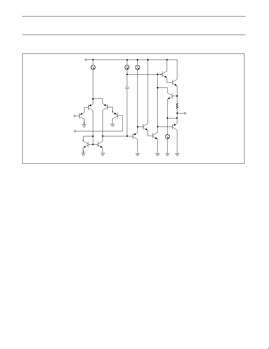
EQUIVALENT CIRCUIT
v+
6
µ
A
100
µ
A
Q2
Q3
Q1
Q4
INPUTS
+
Q8
Q9
CC
Q10
Q5
Q7
Q6
RSC
OUTPUT
Q13
Q12
Q11
SL00066
6
µ
A
50
µ
A
Figure 2. Equivalent circuit.
Philips Semiconductors
Product data
LM124/224/324/324A/
SA534/LM2902
Low power quad op amps
2003 Sep 19
7
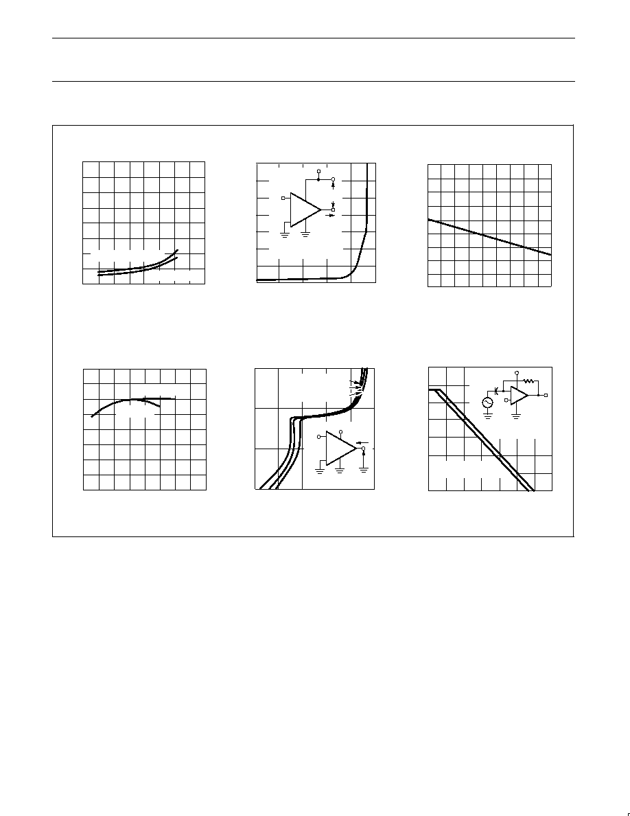
TYPICAL PERFORMANCE CHARACTERISTICS
OP05450S
OP05460S
OP05470S
OP05480S
OP05490S
OP05500S
SUPPL
Y
CURRENT
DRAIN (mAdc)
T
amb
= 0
°
C to +125
°
C
T
amb
= 55
°
C
4
3
2
1
0
0
10
20
30
40
SUPPLY VOLTAGE (V
DC
)
V OUTPUT
VOL
T
AGE
REFERENCE
T
O
V+ (V )
DC
+V+
/2
V+
V2
IO
INDEPENDENT OF V+
T
amb
= +25
o
C
8
7
6
5
4
3
2
1
0.001
0.01
0.1
1
10
100
I
O
+
OUTPUT SOURCE CURRENT (mA
DC
)
+
OUTPUT CURRENT
(mAdc)
90
80
70
60
50
40
30
20
10
0
55 35 15
5
25
45 65
85 105 125
TEMPERATURE (
°
C)
A
-- VOL
T
AGE GAIN (dB)
VOL
VOL
T
AGE GAIN (dB)
+
V
+
10 M
V
O
0.1
µ
f
V
+
/2
V
IN
V
+
= 30 V
DC
AND
55
°
C
T
amb
+125
°
C
V
+
= 10 to 15 V
DC
AND
55
°
C
T
amb
+125
°
C
140
120
100
80
60
40
20
0
1
10
100
1K
10K
100K 1M 10M
FREQUENCY (Hz)
160
120
80
40
0
0
10
20
30
40
SUPPLY VOLTAGE (V
DC
)
RL + 20 k
RL + 2 k
V OUTPUT
VOL
T
AGE (V )
O
DC
V+
/2
V+
V
+
= +5 V
DC
V
+
= +15 V
DC
V
+
= +30 V
DC
10
1
0.1
0.01
0.001
0.01
0.1
1
10
100
I
O
OUTPUT SINK CURRENT (mA
DC
)
V
O
+
Supply Current
Output Characteristics
Current Sourcing
Current Limiting
Voltage Gain
Output Characteristics
Current Sinking
OpenLoop Frequency
Response
SL00067
T
amb
= +25
°
C
I
O
Figure 3. Typical Performance Characteristics
Philips Semiconductors
Product data
LM124/224/324/324A/
SA534/LM2902
Low power quad op amps
2003 Sep 19
8
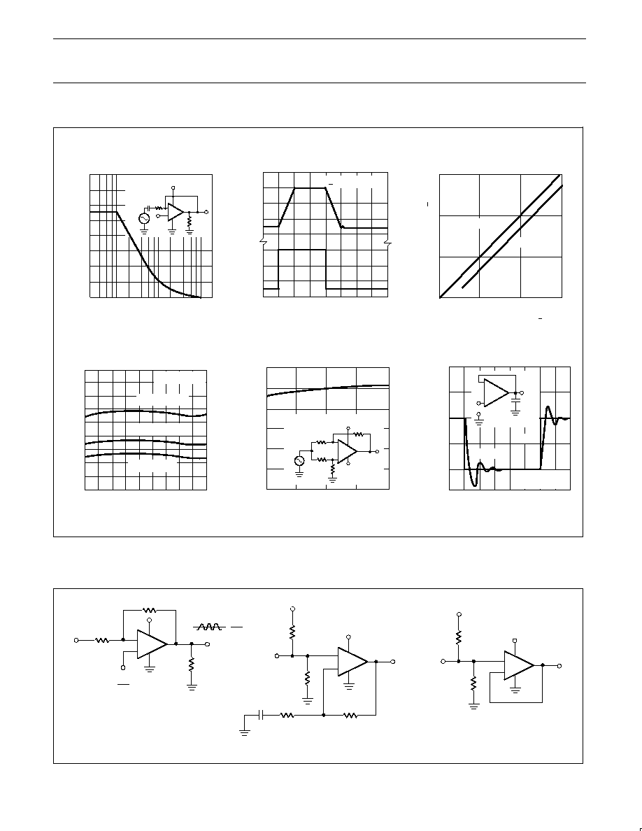
TYPICAL PERFORMANCE CHARACTERISTICS
(Continued)
E OUTPUT
VOL
T
AGE (mV)
O
EO
50pF
INPUT
OUTPUT
500
450
400
350
300
250
0
1
2
3
4
5
6
7
8
L -- TIME (
µ
S)
T
amb
= +25
o
C
V+ = +30 VDC
I INPUT
CURRENT
(nA
)
BD
C
VCM = 0 VDC
V+ = +30 VDC
V+ = +15 VDC
V+ = +5 VDC
90
80
70
60
50
40
30
20
10
0
55 35 15
5
25
45
65
85 105 125
Tamb -- TEMPERATURE (C
o
)
Input Current
V -- OUTPUT
SWING (Vpp)
O
OUTPUT VOL
T
AGE
(V)
INPOUT
VOL
T
AGE (V)
+
VDC
100 k
VO
1 k
+7VDC
VIN
2 k
20
15
10
5
0
1K
10K
100K
1M
FREQUENCY (Hz)
RL < 2K V
+ = 15 VDC
4
3
2
1
0
3
2
1
0
0
10
20
30
40
TIME (
µ
S)
+V -- INPUT
VOL
T
AGE ( V )
IN
DC
+
15
10
5
NEGATIVE
POSITIVE
0
5
10
15
-- POWER SUPPLY VOLTAGE (+ VDC)
V+ OR V
Input Voltage Range
Large-Scale
Frequency Response
Voltage-Follower
Pulse Response
Voltage-Follower Pulse
Response (SmallSignal)
CMRR -- COMMONMODE REJECTION RA
TIO
(dB)
100
100
100k
7.5 VDC
VO
100k
+
+
VIN
+7.5 VDC
120
100
80
60
40
20
0
100
1k
10k
100k
1M
f -- FREQUENCY (Hz)
Common-Mode Rejection Ratio
VIN
SL00068
Figure 4. Typical Performance Characteristics (cont.)
TYPICAL APPLICATIONS
+
V+
8
VO
VIN
+
4
V+
10K
10k
RF
BLOCKS
DC.
GAIN
R1
RF
V+
8
RL
VO
RIN
VIN
+
4
V+
2
V+
8
VO
VIN
4
V+
10K
10k
Single Supply Inverting Amplifier
NonInverting Amplifier
Input Biasing VoltageFollower
V+
2
+
SL00069
Figure 5. Typical Applications
Philips Semiconductors
Product data
LM124/224/324/324A/
SA534/LM2902
Low power quad op amps
2003 Sep 19
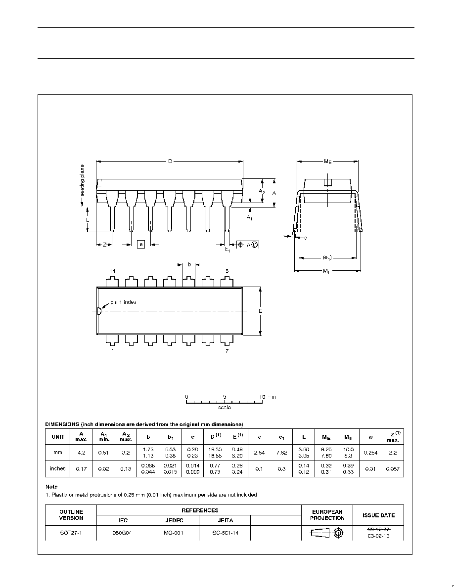
9
DIP14:
plastic dual in-line package; 14 leads (300 mil)
SOT27-1
Philips Semiconductors
Product data
LM124/224/324/324A/
SA534/LM2902
Low power quad op amps
2003 Sep 19
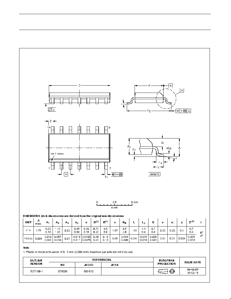
10
SO14:
plastic small outline package; 14 leads; body width 3.9 mm
SOT108-1
Philips Semiconductors
Product data
LM124/224/324/324A/
SA534/LM2902
Low power quad op amps
2003 Sep 19
11
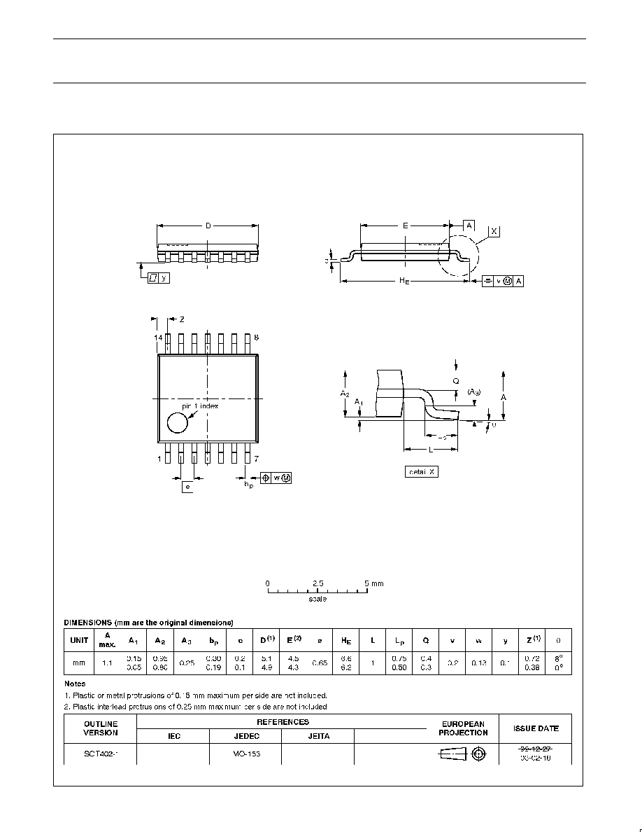
TSSOP14:
plastic thin shrink small outline package; 14 leads; body width 4.4 mm
SOT402-1
Philips Semiconductors
Product data
LM124/224/324/324A/
SA534/LM2902
Low power quad op amps
2003 Sep 19
12
REVISION HISTORY
Rev
Date
Description
_5
20030919
Product data (9397 750 12078). ECN 853-0929 30369 of 19 September 2003.
Modifications:
·
Modified Figure 2; Q10 and Q13 changed from NPN to PNP.
_4
20020712
Product data (9397 750 10172). ECN 853-0929 28616 of 12 July 2002.
Definitions
Short-form specification -- The data in a short-form specification is extracted from a full data sheet with the same type number and title. For detailed information see
the relevant data sheet or data handbook.
Limiting values definition -- Limiting values given are in accordance with the Absolute Maximum Rating System (IEC 60134). Stress above one or more of the limiting
values may cause permanent damage to the device. These are stress ratings only and operation of the device at these or at any other conditions above those given
in the Characteristics sections of the specification is not implied. Exposure to limiting values for extended periods may affect device reliability.
Application information -- Applications that are described herein for any of these products are for illustrative purposes only. Philips Semiconductors make no
representation or warranty that such applications will be suitable for the specified use without further testing or modification.
Disclaimers
Life support -- These products are not designed for use in life support appliances, devices, or systems where malfunction of these products can reasonably be
expected to result in personal injury. Philips Semiconductors customers using or selling these products for use in such applications do so at their own risk and agree
to fully indemnify Philips Semiconductors for any damages resulting from such application.
Right to make changes -- Philips Semiconductors reserves the right to make changes in the products--including circuits, standard cells, and/or software--described
or contained herein in order to improve design and/or performance. When the product is in full production (status `Production'), relevant changes will be communicated
via a Customer Product/Process Change Notification (CPCN). Philips Semiconductors assumes no responsibility or liability for the use of any of these products, conveys
no license or title under any patent, copyright, or mask work right to these products, and makes no representations or warranties that these products are free from patent,
copyright, or mask work right infringement, unless otherwise specified.
Contact information
For additional information please visit
http://www.semiconductors.philips.com.
Fax: +31 40 27 24825
For sales offices addresses send e-mail to:
sales.addresses@www.semiconductors.philips.com.
©
Koninklijke Philips Electronics N.V. 2003
All rights reserved. Printed in U.S.A.
Date of release: 09-03
Document order number:
9397 750 12078
Philips
Semiconductors
Data sheet status
[1]
Objective data
Preliminary data
Product data
Product
status
[2] [3]
Development
Qualification
Production
Definitions
This data sheet contains data from the objective specification for product development.
Philips Semiconductors reserves the right to change the specification in any manner without notice.
This data sheet contains data from the preliminary specification. Supplementary data will be published
at a later date. Philips Semiconductors reserves the right to change the specification without notice, in
order to improve the design and supply the best possible product.
This data sheet contains data from the product specification. Philips Semiconductors reserves the
right to make changes at any time in order to improve the design, manufacturing and supply. Relevant
changes will be communicated via a Customer Product/Process Change Notification (CPCN).
Data sheet status
[1] Please consult the most recently issued data sheet before initiating or completing a design.
[2] The product status of the device(s) described in this data sheet may have changed since this data sheet was published. The latest information is available on the Internet at URL
http://www.semiconductors.philips.com.
[3] For data sheets describing multiple type numbers, the highest-level product status determines the data sheet status.
Level
I
II
III
Document Outline
- DESCRIPTION
- UNIQUE FEATURES
- FEATURES
- PIN CONFIGURATION
- ORDERING INFORMATION
- ABSOLUTE MAXIMUM RATINGS
- DC ELECTRICAL CHARACTERISTICS
- EQUIVALENT CIRCUIT
- TYPICAL PERFORMANCE CHARACTERISTICS
- TYPICAL APPLICATIONS
- PACKAGE OUTLINE
- SOT27-1
- SOT108-1
- SOT402-1
- REVISION HISTORY
- Data sheet status
- Definitions
- Disclaimers