Philips Semiconductors
Product data
LM139/239/239A/339/339A/
LM2901/MC3302
Quad voltage comparator
2
2002 Sep 17
853-0930 28955
DESCRIPTION
The LM139 series consists of four independent precision voltage
comparators, with an offset voltage specification as low as 2.0 mV
max for each comparator, which were designed specifically to
operate from a single power supply over a wide range of voltages.
Operation from split power supplies is also possible and the low
power supply current drain is independent of the magnitude of the
power supply voltage. These comparators also have a unique
characteristic in that the input common-mode voltage range includes
ground, even though they are operated from a single power supply
voltage.
The LM139 series was designed to directly interface with TTL and
CMOS. When operated from both plus and minus power supplies,
the LM139 series will directly interface with MOS logic where their
low power drain is a distinct advantage over standard comparators.
FEATURES
∑
Wide single supply voltage range 2.0 V
DC
to 32 V
DC
or dual
supplies
±
1.0 V
DC
to
±
16 V
DC
∑
Very low supply current drain (0.8 mA) independent of supply
voltage (1.0 mW/comparator at 5.0 V
DC
)
∑
Low input biasing current 25 nA
∑
Low input offset current
±
5 nA and offset voltage
∑
Input common-mode voltage range includes ground
∑
Differential input voltage range equal to the power supply voltage
∑
Low output 250 mV at 4 mA saturation voltage
∑
Output voltage compatible with TTL, DTL, ECL, MOS and CMOS
logic systems
APPLICATIONS
∑
A/D converters
∑
Wide range VCO
∑
MOS clock generator
∑
High voltage logic gate
∑
Multivibrators
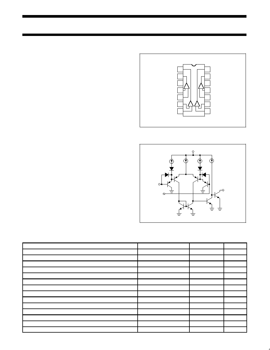
PIN CONFIGURATION
1
2
3
4
5
6
7
8
14
13
12
11
10
9
OUTPUT 2
OUTPUT 1
V+
INPUT 1 ≠
INPUT 1 +
OUTPUT 3
TOP VIEW
D, DH, and N Packages
INPUT 1 ≠
INPUT 1 +
OUTPUT 4
GND
INPUT 4 ≠
INPUT 3 +
INPUT 3 ≠
INPUT 4 +
1
2
3
4
SL00070
Figure 1. Pin Configuration
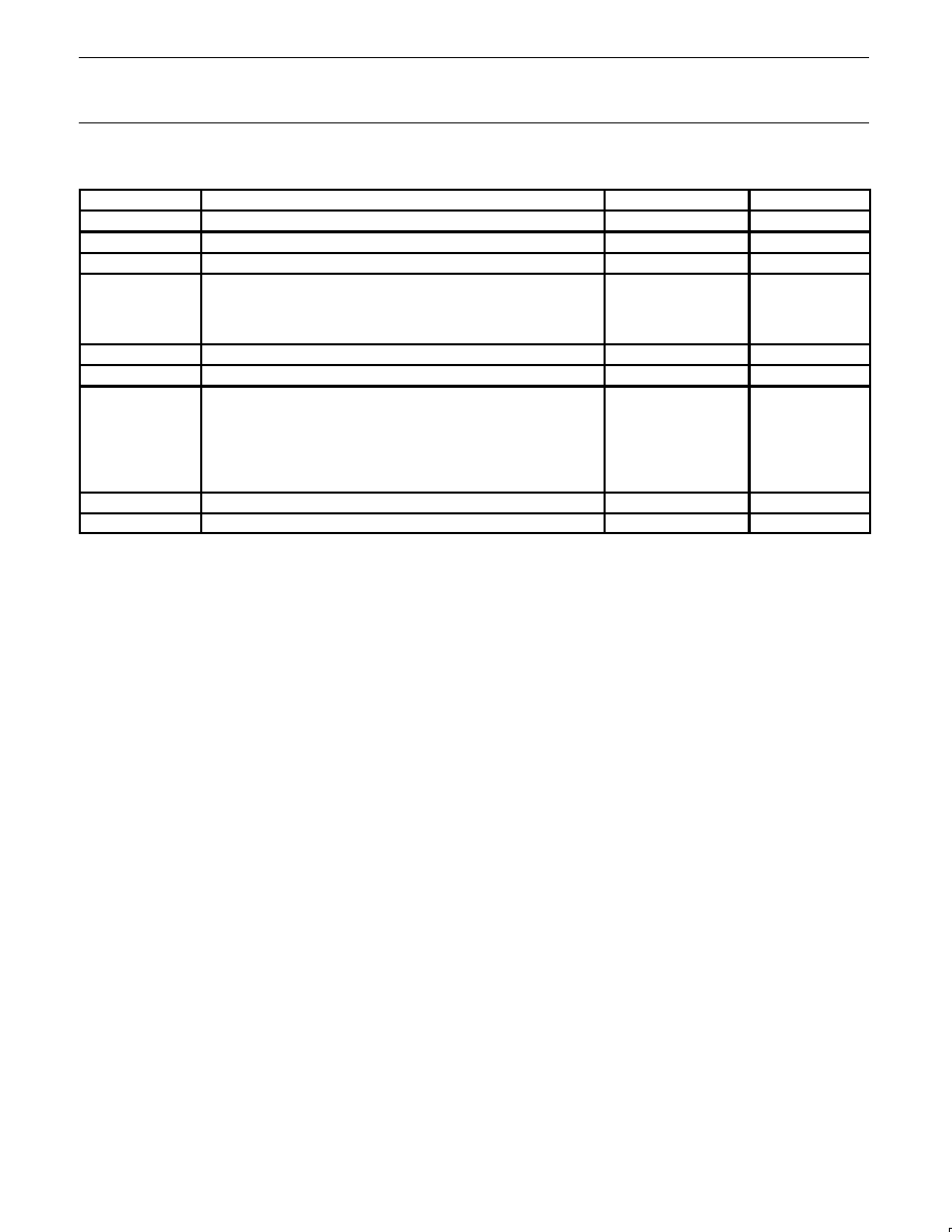
EQUIVALENT CIRCUIT
V +
100
µ
A
3.5
µ
A
3.5
µ
A
100
µ
A
Q1
Q2
Q3
Q4
Q8
Q7
Q6
Q5
≠ INPUT
OUTPUT
+ INPUT
(1 Comparator Only)
SL00071
Figure 2. Equivalent Circuit
ORDERING INFORMATION
DESCRIPTION
TEMPERATURE RANGE
ORDER CODE
DWG #
14-Pin Plastic Dual In-Line Package (DIP)
≠55
∞
C to +125
∞
C
LM139N
SOT27-1
14-Pin Plastic Small Outline (SO) Package
≠25
∞
C to +85
∞
C
LM239D
SOT108-1
14-Pin Plastic Dual In-Line Package (DIP)
≠25
∞
C to +85
∞
C
LM239N
SOT27-1
14-Pin Plastic Dual In-Line Package (DIP)
≠25
∞
C to +85
∞
C
LM239AN
SOT27-1
14-Pin Plastic Small Outline (SO) Package
≠40
∞
C to +125
∞
C
LM2901D
SOT108-1
14-Pin Plastic Dual In-Line Package (DIP)
≠40
∞
C to +125
∞
C
LM2901N
SOT27-1
14-Pin Plastic Thin Shrink Small Outline Package (TSSOP)
≠40
∞
C to +125
∞
C
LM2901DH
SOT402-1
14-Pin Plastic Small Outline (SO) Package
0
∞
C to +70
∞
C
LM339AD
SOT108-1
14-Pin Plastic Dual In-Line Package (DIP)
0
∞
C to +70
∞
C
LM339AN
SOT27-1
14-Pin Plastic Small Outline (SO) Package
0
∞
C to +70
∞
C
LM339D
SOT108-1
14-Pin Plastic Thin Shrink Small Outline Package (TSSOP)
0
∞
C to +70
∞
C
LM339DH
SOT402-1
14-Pin Plastic Dual In-Line Package (DIP)
0
∞
C to +70
∞
C
LM339N
SOT27-1
14-Pin Plastic Small Outline (SO) Package
≠40
∞
C to +85
∞
C
MC3302D
SOT108-1
14-Pin Plastic Dual In-Line Package (DIP)
≠40
∞
C to +85
∞
C
MC3302N
SOT27-1
Philips Semiconductors
Product data
LM139/239/239A/339/339A/
LM2901/MC3302
Quad voltage comparator
2002 Sep 17
3
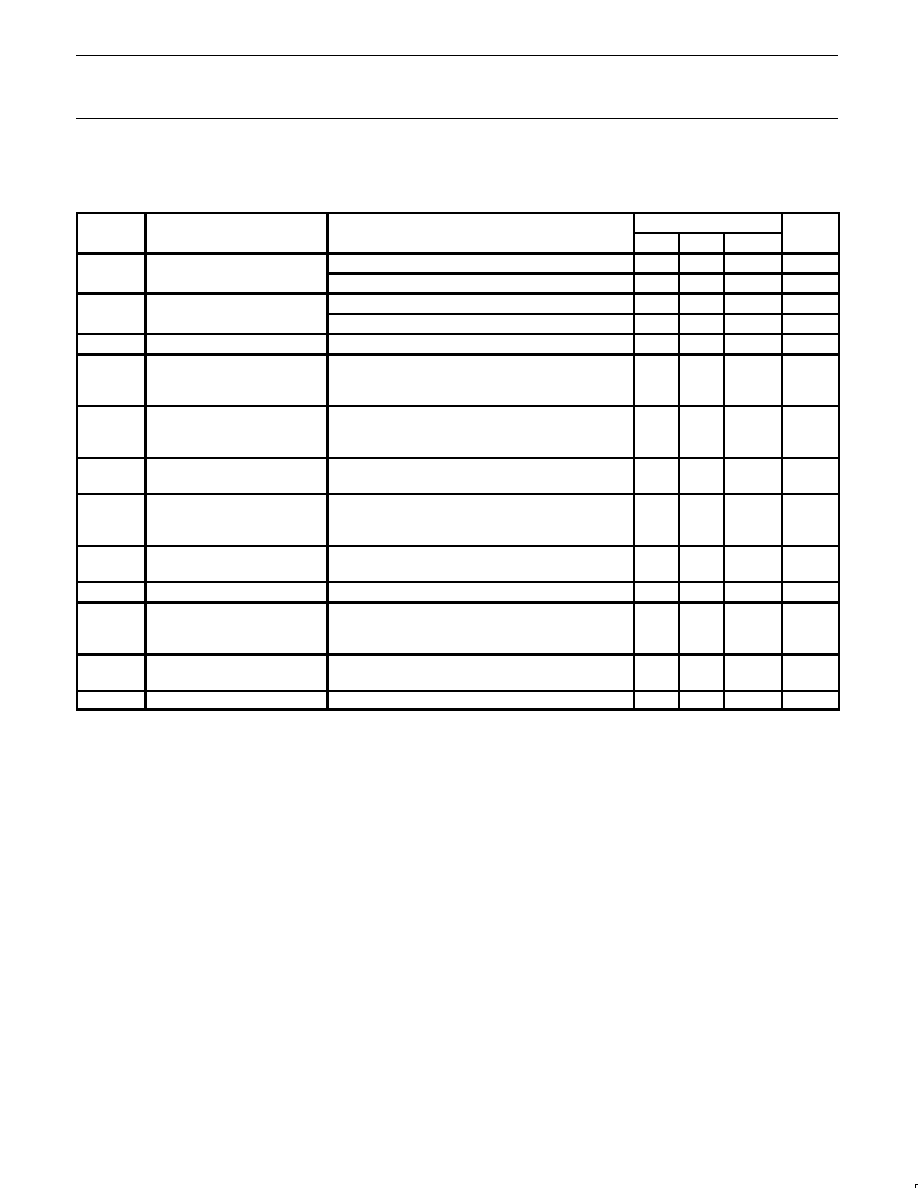
ABSOLUTE MAXIMUM RATINGS
SYMBOL
PARAMETER
RATING
UNIT
V
CC
V
CC
supply voltage
32 or
±
16
V
DC
V
DIFF
Differential input voltage
32
V
DC
V
IN
Input voltage
≠0.3 to +32
V
DC
P
D
Maximum power dissipation, T
amb
= 25
∞
C (still≠air)
1
N package
1420
mW
D package
1040
mW
DH package
762
mW
Output short-circuit to ground
2
Continuous
I
IN
Input current (V
IN
< ≠0.3 V
DC
)
3
50
mA
T
amb
Operating temperature range
LM139
≠55 to +125
∞
C
LM239/239A
≠25 to +85
∞
C
LM339/339A
0 to +70
∞
C
LM2901
≠40 to +125
∞
C
MC3302
≠40 to +85
∞
C
T
stg
Storage temperature range
≠65 to +150
∞
C
T
sld
Lead soldering temperature (10 sec max)
230
∞
C
NOTES:
1.
Derate above 25
∞
C,
at the following rates:
N Package at 11.4 mW/
∞
C
D Package at 8.3 mW/
∞
C
DH Package at 6.1 mW/
∞
C
2. Short circuits from the output to V+ can cause excessive heating and eventual destruction. The maximum output current is approximately
20 mA independent of the magnitude of V+.
3. This input current will only exist when the voltage at any of the input leads is driven negative. It is due to the collector≠base junction of
the input PNP transistors becoming forward biased and thereby acting as input diode clamps. In addition to this diode action, there is also
lateral NPN parasitic transistor action on the IC chip. This transistor action can cause the output voltages of the comparators to go to the V+
voltage level (or to ground for a large overdrive) for the time duration that an input is driven negative. This is not destructive and normal
output states will reestablish when the input voltage, which was negative, again returns to a value greater than ≠0.3 V
DC
.
Philips Semiconductors
Product data
LM139/239/239A/339/339A/
LM2901/MC3302
Quad voltage comparator
2002 Sep 17
4
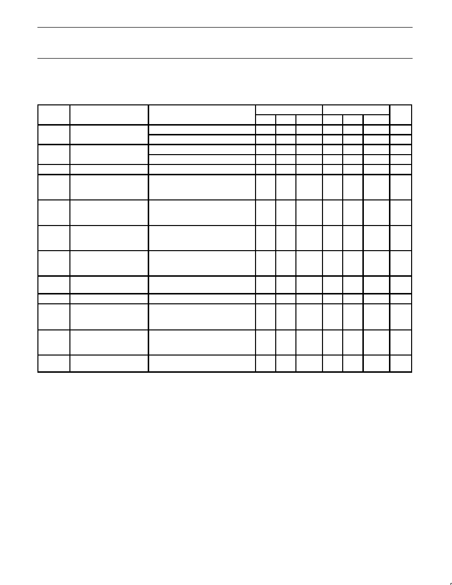
DC AND AC ELECTRICAL CHARACTERISTICS
V+ = 5 V
DC
; LM139: ≠55
∞
C
T
amb
+125
∞
C; LM239/239A: ≠25
∞
C
T
amb
+85
∞
C; LM339/339A: 0
∞
C
T
amb
+70
∞
C;
LM2901: ≠40
∞
C
T
amb
+125
∞
C; MC3302: ≠40
∞
C
T
amb
+85
∞
C, unless otherwise specified.
SYMBOL
PARAMETER
TEST CONDITIONS
LM239A/339A
UNIT
SYMBOL
PARAMETER
TEST CONDITIONS
Min
Typ
Max
UNIT
V
OS
Input offset voltage
2
T
amb
= 25
∞
C
±
1.0
±
2.0
mV
V
OS
Input offset voltage
2
Over temp.
±
4.0
mV
V
C
Input common-mode voltage
T
amb
= 25
∞
C
0
V+ ≠1.5
V
V
CM
g
range
3
Over temp.
0
V+ ≠2.0
V
V
IDR
Differential input voltage
1
Keep all V
IN
0 V
DC
(or V≠ if needed)
V+
V
4
I
IN(+)
or I
IN(≠)
with output in linear range
I
BIAS
Input bias current
4
T
amb
= 25
∞
C
25
250
nA
Over temp.
400
nA
I
IN(+)
≠ I
IN(≠)
I
OS
Input offset current
T
amb
= 25
∞
C
±
5.0
±
50
nA
Over temp.
±
150
nA
I
OL
Output sink current
V
IN(≠)
1 V
DC
; V
IN
(+) = 0; V
O
1.5 V
DC
;
T
amb
= 25
∞
C
6.0
16
mA
V
IN(+)
1 V
DC
; V
IN
(≠) = 0
Output leakage current
V
O
= 5 V
DC
; T
amb
= 25
∞
C
0.1
nA
V
O
= 30 V
DC
; over temp.
1.0
µ
A
I
CC
Supply current
R
L
=
on comparators; V+ = 30 V;
T
amb
= 25
∞
C
0.8
2.0
mA
A
V
Voltage gain
R
L
15 k
; V+ = 15 V
DC
50
200
V/mV
V
IN(≠)
1 V
DC
; V
IN(+)
= 0; I
SINK
4 mA
V
OL
Saturation voltage
T
amb
= 25
∞
C
250
400
mV
Over temp.
700
mV
t
LSR
Large-signal response time
V
IN
= TTL logic swing; V
REF
= 1.4 V
DC
; V
RL
= 5 V
DC
;
R
L
= 5.1 k
; T
amb
= 25
∞
C
300
ns
t
R
Response time
5
V
RL
= 5 V
DC
; R
L
= 5.1 k
; T
amb
= 25
∞
C
1.3
µ
s
See notes at the end of the Electrical Characteristics.
Philips Semiconductors
Product data
LM139/239/239A/339/339A/
LM2901/MC3302
Quad voltage comparator
2002 Sep 17
5
DC AND AC ELECTRICAL CHARACTERISTICS (continued)
V+ = 5 V
DC
; LM139: ≠55
∞
C
T
amb
+125
∞
C; LM239/239A: ≠25
∞
C
T
amb
+85
∞
C; LM339/339A: 0
∞
C
T
amb
+70
∞
C;
LM2901: ≠40
∞
C
T
amb
+125
∞
C; MC3302: ≠40
∞
C
T
amb
+85
∞
C, unless otherwise specified.
SYMBOL
PARAMETER
TEST CONDITIONS
LM139
LM239/339
UNIT
SYMBOL
PARAMETER
TEST CONDITIONS
Min
Typ
Max
Min
Typ
Max
UNIT
V
OS
Input offset voltage
2
T
amb
= 25
∞
C
±
2.0
±
5.0
±
2.0
±
5.0
mV
V
OS
Input offset voltage
2
Over temp.
±
9.0
±
9.0
mV
V
C
Input common-mode
T
amb
= 25
∞
C
0
V+≠1.5
0
V+≠1.5
V
V
CM
voltage range
3
Over temp.
0
V+≠2.0
0
V+≠2.0
V
V
IDR
Differential input voltage
1
Keep all V
IN
0 V
DC
(or V≠ if needed)
V+
V+
V
4
I
IN(+)
or I
IN(≠)
with output in linear range
I
BIAS
Input bias current
4
T
amb
= 25
∞
C
25
100
25
250
nA
Over temp.
300
400
nA
I
IN(+)
≠ I
IN(≠)
I
OS
Input offset current
T
amb
= 25
∞
C
±
3.0
±
25
±
5.0
±
50
nA
Over temp.
±
100
±
150
nA
I
OL
Output sink current
V
IN(≠)
1 V
DC
; V
IN(+)
= 0;
V
O
1.5 V
DC
;
T
amb
= 25
∞
C
6.0
16
6.0
16
mA
V
IN(+)
1 V
DC
; V
IN(≠)
= 0
Output leakage current
V
O
= 5 V
DC
; T
amb
= 25
∞
C
0.1
0.1
nA
V
O
= 30 V
DC
; Over temp.
1.0
1.0
µ
A
I
CC
Supply current
R
L
=
on comparators; V+ = 30 V;
T
amb
= 25
∞
C
0.8
2.0
0.8
2.0
mA
A
V
Voltage gain
R
L
15 k
; V+ = 15 V
DC
50
200
50
200
V/mV
V
OL
Saturation voltage
V
IN(≠)
1 V
DC
; V
IN(+)
= 0; I
SINK
4 mA
T
amb
= 25
∞
C
250
400
250
400
mV
Over temp.
700
700
mV
t
LSR
Large-signal response time
V
IN
= TTL logic swing; V
REF
= 1.4 V
DC
;
V
RL
= 5 V
DC
; R
L
= 5.1 k
;
T
amb
= 25
∞
C
300
300
ns
t
R
Response time
5
V
RL
= 5 V
DC
; R
L
= 5.1 k
;
T
amb
= 25
∞
C
1.3
1.3
µ
s
See notes on following page.
