 | ÐлекÑÑоннÑй компоненÑ: LM139N | СкаÑаÑÑ:  PDF PDF  ZIP ZIP |
Äîêóìåíòàöèÿ è îïèñàíèÿ www.docs.chipfind.ru
Philips
Semiconductors
LM139/239/239A/339/339A/LM2901/MC
3302
Quad voltage comparator
Product specification
1995 Nov 27
INTEGRATED CIRCUITS
IC11 Data Handbook
Philips Semiconductors
Product specification
LM139/239/239A/339/339A
/LM2901/MC3302
Quad voltage comparator
2
1995 Nov 27
853-0930 16050
DESCRIPTION
The LM139 series consists of four independent precision voltage
comparators, with an offset voltage specification as low as 2.0mV
max for each comparator, which were designed specifically to
operate from a single power supply over a wide range of voltages.
Operation from split power supplies is also possible and the low
power supply current drain is independent of the magnitude of the
power supply voltage. These comparators also have a unique
characteristic in that the input commonmode voltage range
includes ground, even though they are operated from a single power
supply voltage.
The LM139 series was designed to directly interface with TTL and
CMOS. When operated from both plus and minus power supplies,
the LM139 series will directly interface with MOS logic where their
low power drain is a distinct advantage over standard comparators.
FEATURES
·
Wide single supply voltage range 2.0V
DC
to 36V
DC
or dual
supplies
±
1.0V
DC
to
±
18V
DC
·
Very low supply current drain (0.8mA) independent of supply
voltage (1.0mW/comparator at 5.0V
DC
)
·
Low input biasing current 25nA
·
Low input offset current
±
5nA and offset voltage
·
Input commonmode voltage range includes ground
·
Differential input voltage range equal to the power supply voltage
·
Low output 250mV at 4mA saturation voltage
·
Output voltage compatible with TTL, DTL, ECL, MOS and CMOS
logic systems
APPLICATIONS
·
A/D converters
·
Wide range VCO
·
MOS clock generator
·
High voltage logic gate
·
Multivibrators
PIN CONFIGURATION
1
2
3
4
5
6
7
8
14
13
12
11
10
9
OUTPUT 2
OUTPUT 1
V+
INPUT 1
INPUT 1 +
OUTPUT 3
TOP VIEW
D, F, N Packages
INPUT 1
INPUT 1 +
OUTPUT 4
GND
INPUT 4
INPUT 3 +
INPUT 3
INPUT 4 +
1
2
3
4
SL00070
Figure 1. Pin Configuration
EQUIVALENT CIRCUIT
V +
100
µ
A
3.5
µ
A
3.5
µ
A
100
µ
A
Q1
Q2
Q3
Q4
Q8
Q7
Q6
Q5
INPUT
OUTPUT
+ INPUT
(1 Comparator Only)
SL00071
Figure 2. Equivalent Circuit
ORDERING INFORMATION
DESCRIPTION
TEMPERATURE RANGE
ORDER CODE
DWG #
14Pin Ceramic Dual In-Line Package (Cerdip)
55 to +125
°
C
LM139F
0581B
14Pin Plastic Dual In-Line Package (DIP)
25
°
C to +85
°
C
LM239AN
SOT27-1
14Pin Plastic Dual In-Line Package (DIP)
25
°
C to +85
°
C
LM239N
SOT27-1
14Pin Plastic Small Outline (SO) Package
25
°
C to +85
°
C
LM239D
SOT108-1
14Pin Plastic Dual In-Line Package (DIP)
40
°
C to +125
°
C
LM2901N
SOT27-1
14Pin Plastic Small Outline (SO) Package
40
°
C to +125
°
C
LM2901D
SOT108-1
14Pin Plastic Dual In-Line Package (DIP)
0 to +70
°
C
LM339AN
SOT27-1
14Pin Plastic Small Outline (SO) Package
0 to +70
°
C
LM339D
SOT108-1
14Pin Plastic Dual In-Line Package (DIP)
0 to +70
°
C
LM339N
SOT27-1
14Pin Plastic Small Outline (SO) Package
40
°
C to +85
°
C
MC3302D
SOT108-1
14Pin Ceramic Dual In-Line Package (Cerdip)
40
°
C to +85
°
C
MC3302F
0581B
14Pin Plastic Dual In-Line Package (DIP)
40
°
C to +85
°
C
MC3302N
SOT27-1
14Pin Plastic Dual In-Line Package (DIP)
55 to +125
°
C
LM139N
SOT27-1
Philips Semiconductors
Product specification
LM139/239/239A/339/339A/
LM2901/MC3302
Quad voltage comparator
1995 Nov 27
3
ABSOLUTE MAXIMUM RATINGS
SYMBOL
PARAMETER
RATING
UNIT
V
CC
V
CC
supply voltage
36 or
±
18
V
DC
V
DIFF
Differential input voltage
36
V
DC
V
IN
Input voltage
0.3 to +36
V
DC
P
D
Maximum power dissipation,
T
A
=25
°
C (stillair)
1
F package
1190
mW
N package
1420
mW
D package
1040
mW
Output shortcircuit to ground
2
Continuous
I
IN
Input current (V
IN
<0.3V
DC
)
3
50
mA
T
A
Operating temperature range
LM139
55 to +125
°
C
LM239/239A
25 to +85
°
C
LM339/339A
0 to +70
°
C
LM2901
40 to +125
°
C
MC3302
40 to +85
°
C
T
STG
Storage temperature range
65 to +150
°
C
T
SOLD
Lead soldering temperature (10sec max)
300
°
C
NOTES:
1.
Derate above 25
°
C,
at the following rates:
F Package at 9.5mW/
°
C
N Package at 11.4mW/
°
C
D Package at 8.3mW/
°
C
2. Short circuits from the output to V+ can cause excessive heating and eventual destruction. The maximum output current is approximately
20mA independent of the magnitude of V+.
3. This input current will only exist when the voltage at any of the input leads is driven negative. It is due to the collectorbase junction of the
input PNP transistors becoming forward biased and thereby acting as input diode clamps. In addition to this diode action, there is also lateral
NPN parasitic transistor action on the IC chip. This transistor action can cause the output voltages of the comparators to go to the V+ voltage
level (or to ground for a large overdrive) for the time duration that an input is driven negative. This is not destructive and normal output states
will reestablish when the input voltage, which was negative, again returns to a value greater than 0.3V
DC
.
Philips Semiconductors
Product specification
LM139/239/239A/339/339A/
LM2901/MC3302
Quad voltage comparator
1995 Nov 27
4
DC AND AC ELECTRICAL CHARACTERISTICS
V+=5V
DC
, LM139: 55
°
C
T
A
125
°
C; LM239/239A: 25
°
C
T
A
85
°
C; LM339/339A: 0
°
C
T
A
70
°
C;; LM2901: 40
°
C
T
A
125
°
C,
MC3302: 40
°
C
T
A
85
°
C, unless otherwise specified.
SYMBOL
PARAMETER
TEST CONDITIONS
LM239A/339A
UNIT
SYMBOL
PARAMETER
TEST CONDITIONS
Min
Typ
Max
UNIT
V
OS
Input offset voltage
2
T
A
=25
°
C
Over temp.
±
1.0
±
2.0
±
4.0
mV
mV
V
CM
Input commonmode voltage
range
3
T
A
=25
°
C
Over temp.
0
0
V+1.5
V+2.0
V
V
IDR
Differential input voltage
1
Keep all
V
IN
s
0V
DC
(or V if need)
V+
V
I
BIAS
Input bias current
4
I
IN(+)
or I
IN()
with output in
linear range
T
A
=25
°
C
Over temp.
25
250
400
nA
nA
I
IN(+)
I
IN()
I
OS
Input offset current
T
A
=25
°
C
±
5.0
±
50
nA
Over temp.
±
150
nA
I
OL
Output sink current
V
IN()
1V
DC
, V
IN
(+)=0,
V
O
1.5V
DC
,
T
A
=25
°
C
6.0
16
mA
V
IN(+)
1V
DC
, V
IN
()=0
Output leakage current
V
O
=5V
DC
, T
A
=25
°
C
0.1
nA
V
O
=30V
DC
, over temp.
1.0
µ
A
I
CC
Supply current
R
L
=
on comparators,
T
A
=25
°
C
V+=30V
0.8
2.0
mA
A
V
Voltage gain
R
L
15k
,
V+=15V
DC
50
200
V/mV
V
OL
Saturation voltage
V
IN()
1V
DC
, V
IN(+)
=0,
I
SINK
4mA
T
A
=25
°
C
Over temp.
250
400
700
mV
mV
t
LSR
Largesignal response time
V
IN
=TTL logic swing, V
REF
=1.4V
DC
, V
RL
=5V
DC
,
R
L
=5.1k
, T
A
=25
°
C
300
ns
t
R
Response time
5
V
RL
=5V
DC
, R
L
=5.1k
,
T
A
=25
°
C
1.3
µ
s
See notes at the end of the Electrical Characteristics.
Philips Semiconductors
Product specification
LM139/239/239A/339/339A/
LM2901/MC3302
Quad voltage comparator
1995 Nov 27
5
DC AND AC ELECTRICAL CHARACTERISTICS
V+=5V
DC
, LM139: 55
°
C
T
A
125
°
C; LM239/239A: 25
°
C
T
A
85
°
C; LM339/339A: 0
°
C
T
A
70
°
C; LM2901: 40
°
C
T
A
125
°
C,
MC3302: 40
°
C
T
A
85
°
C, unless otherwise specified.
SYMBOL
PARAMETER
TEST CONDITIONS
LM139
LM239/339
UNIT
SYMBOL
PARAMETER
TEST CONDITIONS
Min
Typ
Max
Min
Typ
Max
UNIT
V
OS
Input offset voltage
2
T
A
=25
°
C
Over temp.
±
2.0
±
5.0
±
9.0
±
2.0
±
5.0
±
9.0
mV
mV
V
CM
Input commonmode voltage
range
3
T
A
=25
°
C
Over temp.
0
0
V+1.5
V+2.0
0
0
V+1.5
V+2.0
V
V
IDR
Differential input voltage
1
Keep all
V
IN
s
0V
DC
(or V if need)
V+
V+
V
I
BIAS
Input bias current
4
I
IN(+)
or I
IN()
with output in
linear range
T
A
=25
°
C
Over temp.
25
100
300
25
250
400
nA
nA
I
IN(+)
I
IN()
I
OS
Input offset current
T
A
=25
°
C
±
3.0
±
25
±
5.0
±
50
nA
Over temp.
±
100
±
150
nA
I
OL
Output sink current
V
IN()
1V
DC
, V
IN
(+)=0,
V
O
1.5V
DC
,
T
A
=25
°
C
6.0
16
6.0
16
mA
V
IN(+)
1V
DC
, V
IN
()=0
V
O
=5V
DC
,
Output leakage current
T
A
=25
°
C
0.1
0.1
nA
V
O
=30V
DC
,
over temp.
1.0
1.0
µ
A
I
CC
Supply current
R
L
=
on comparators,
T
A
=25
°
C
V+=30V
0.8
2.0
0.8
2.0
mA
A
V
Voltage gain
R
L
15k
,
V+=15V
DC
50
200
50
200
V/mV
V
OL
Saturation voltage
V
IN()
1V
DC
, V
IN(+)
=0,
I
SINK
4mA
T
A
=25
°
C
Over temp.
250
400
700
250
400
700
mV
mV
t
LSR
Largesignal response time
V
IN
=TTL logic swing, V
REF
=1.4V
DC
,
V
RL
=5V
DC
, R
L
=5.1k
, T
A
=25
°
C
300
300
ns
t
R
Response time
5
V
RL
=5V
DC
, R
L
=5.1k
,
T
A
=25
°
C
1.3
1.3
µ
s
See notes on following page.
Philips Semiconductors
Product specification
LM139/239/239A/339/339A/
LM2901/MC3302
Quad voltage comparator
1995 Nov 27
6
DC AND AC ELECTRICAL CHARACTERISTICS
V+=5V
DC
, LM139: 55
°
C
T
A
125
°
C; LM239/239A: 25
°
C
T
A
85
°
C; LM339/339A: 0
°
C
T
A
70
°
C; LM2901: 40
°
C
T
A
125
°
C,
MC3302: 40
°
C
T
A
85
°
C, unless otherwise specified.
SYMBOL
PARAMETER
TEST CONDITIONS
LM2901
MC3302
UNIT
SYMBOL
PARAMETER
TEST CONDITIONS
Min
Typ
Max
Min
Typ
Max
UNIT
V
OS
Input offset voltage
2
T
A
=25
°
C
Over temp.
±
2.0
±
9
±
7.0
±
15
±
3.0
±
20
±
40
mV
mV
V
CM
Input commonmode voltage
range
3
T
A
=25
°
C
Over temp.
0
0
V+1.5
V+2.0
0
0
V+1.5
V+2.0
V
V
IDR
Differential input voltage
1
Keep all
V
IN
s
0V
DC
(or V if need)
V+
V+
V
I
BIAS
Input bias current
4
I
IN(+)
or I
IN()
with output in
linear range
T
A
=25
°
C
Over temp.
25
200
250
500
25
500
1000
nA
nA
I
IN(+)
I
IN()
I
OS
Input offset current
T
A
=25
°
C
±
5
±
50
±
5
±
100
nA
Over temp.
±
50
±
200
±
300
nA
I
OL
Output sink current
V
IN()
1V
DC
, V
IN
(+)=0,
V
O
1.5V
DC
,
T
A
=25
°
C
6.0
16
6
16
mA
V
IN(+)
1V
DC
, V
IN
()=0
V
O
=5V
DC
,
Output leakage current
T
A
=25
°
C
0.1
0.1
nA
V
O
=30V
DC
,
over temp.
1.0
1.0
µ
A
R
L
=
on all comparators,
.8
1.8
mA
I
CC
Supply current
T
A
=25
°
C
0.8
2.0
R
L
=
on all comparators, V+=30V
1.0
2.5
mA
A
V
Voltage gain
R
L
15k
,
V+=15V
DC
25
100
2
100
V/mV
V
OL
Saturation voltage
V
IN()
1V
DC
, V
IN(+)
=0,
I
SINK
4mA
T
A
=25
°
C
Over temp.
400
400
700
150
400
700
mV
mV
t
LSR
Largesignal response time
V
IN
=TTL logic swing, V
REF
=1.4V
DC
,
V
RL
=5V
DC
, R
L
=5.1k
, T
A
=25
°
C
300
300
ns
t
R
Response time
5
V
RL
=5V
DC
, R
L
=5.1k
,
T
A
=25
°
C
1.3
1.3
µ
s
NOTES:
1. Positive excursions of input voltage may exceed the power supply level by 17V. As long as the other voltage remains within the
common-mode range, the comparator will provide a proper output state. The low input voltage state must not be less than 0.3V
DC
(or
0.3V
DC
below the magnitude of the negative power supply, if used).
2. At output switch point, V
O
1.4V
DC
, R
S
=0
with V+ from 5V
DC
to 30V
DC
; and over the full input commonmode range (0V
DC
to
V+ 1.5V
DC
). Inputs of unused comparators should be grounded.
3. The input commonmode voltage or either input signal voltage should not be allowed to go negative by more than 0.3V. The upper end of
the commonmode voltage range is V+ 1.5V, but either or both inputs can go to 30V
DC
without damage.
4. The direction of the input current is out of the IC due to the PNP input stage. This current is essentially constant, independent of the state of
the output so no loading change exists on the reference or input lines.
5. The response time specified is for a 100mV input step with a 5mV overdrive. For larger overdrive signals, 300ns can be obtained (see typical
performance characteristics section).
Philips Semiconductors
Product specification
LM139/239/239A/339/339A/
LM2901/MC3302
Quad voltage comparator
1995 Nov 27
7
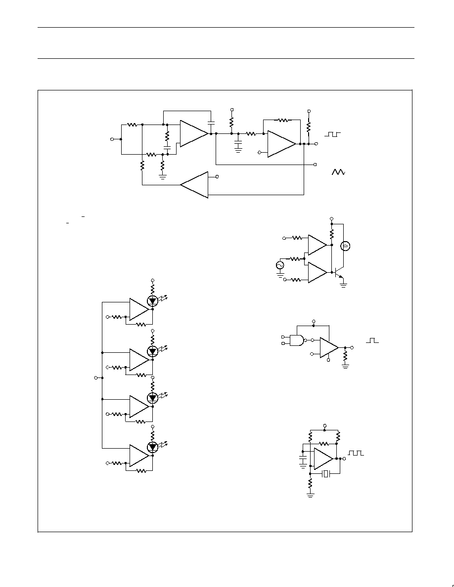
EQUIVALENT CIRCUIT
100k
500pF
10
0.1
µ
F
20k
50k
20k
V + /2
V +
30k
5.1k
700k
V /2
+
+ VC
FREQUENCY
CONTROL
VOLTAGE
INPUT
3.0k
OUTPUT 1
OUTPUT 2
+
+
+ VREF HI
+ VIN
2RS
RS
2RS
+ V (12VDC)
10K
LAMP
2N2222
+
+
+
+ 5VDC
360
100
100k
+
+ 5VDC
360
100
100k
+
+ 5VDC
360
100
100k
+
+ 5VDC
360
100
100k
+ VREF 4
+ VREF 3
+ VREF 2
+ VREF 1
VO
+
V+
2.0k
V+
o
VO
1 100kHz
CRYSTAL
200k
200k
100k
0.1
µ
F
CrystalControlled Oscillator
Limit Comparator
TwoDecade HighFrequency VCO
Visible Voltage Indicator
+
TTLtoMOS Logic Converter
NOTES:
V+ = 30VDC
+ 250m VDC < VC = 50VDC
700H < fO = 100kHz
NOTE:
Input of unused comparators should be grounded.
1/4LM339
1/4LM339
1/4LM339
+ VREF LO
5VDC
12VDC
0.01
µ
F
V+
+ VREF
(1.4V
DC
)
10K
1/4LM339
VO
12V
o
SL00072
Figure 3. Equivalent Circuit
Philips Semiconductors
Product specification
LM139/239/239A/339/339A/
LM2901/MC3302
Quad voltage comparator
1995 Nov 27
8
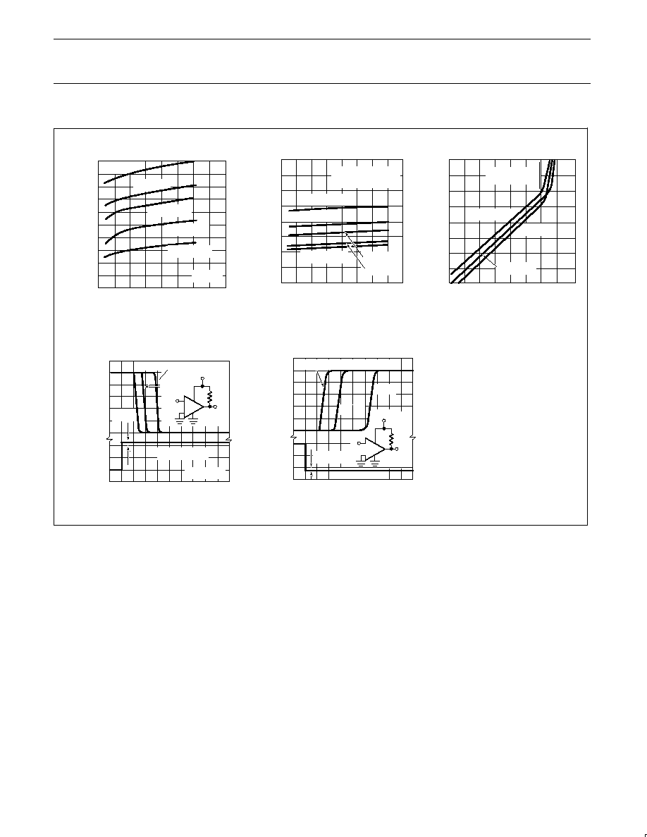
TYPICAL PERFORMANCE CHARACTERISTICS
INPUT VOL
T
AGE
V -- mV
IN
OUTPUT VOL
T
AGE
V -- mV
O
VOUT
VIN
+
+ 5V
1.0
0.8
0.6
0.4
0.2
0
10
20
30
40
V+ -- SUPPLY VOLTAGE -- VDC
I
+
--
SUPPL
Y
CURRENT -- mA
TA -55
o
C
TA = 0
o
C
TA = +25
o
C
TA = 125
o
C
TA = +70
o
C
RL =
80
60
40
20
0
10
20
30
40
v + -- SUPPLY VOLTAGE -- VDC
I -- INPUT CURRENT -- nA ND
C
TA = 55
o
C
TA = 0
o
C
TA = +70
o
C
TA = +25
o
C
TA = +125
o
C
VIN (CM) = 0 VDC
RIN (CM) = 10k
OUT OF
SATURATION
TA =
+125
o
C
TA = 55
o
C
TA
+
25
o
10
1.0
0.1
0.01
0.001
0.01
0.1
1.0
10
100
IO -- OUTPUT SINK CURRENT (mA)
V -- SA
TURA
TION VOL
T
AGE (V )
OD
C
6
5
4
3
2
1
0
0
50
100
0
0.5
1.0
1.5
2.0
TIME --
µ
sec
INPUT VOL
T
AGE
V -- mV
IN
OUTPUT VOL
T
AGE
V -- mV
O
5mV = INPUT OVERDRIVE
100mV
OVERDRIVE
TA = 25
o
C
5.1K
VOUT
VIN
20mV
+
+ 5V
INPUT OVERDRIVE = 100mV
20mV
5mV
OVERDRIVE
6
5
4
3
2
1
0
0
50
100
0
0.5
1.0
1.5
2.0
TIME --
µ
sec
TA = 25
o
C
5.1K
Supply Current
Input Current
Output Saturation Voltage
Response Time for Various
Input Overdrives --
Negative Transition
Response Time for Various
Input Overdrives --
Positive Transition
SL00073
Figure 4. Typical Performance Characteristics

Philips Semiconductors
Product specification
LM139/239/239A/339/339A/
LM2901/MC3302
Quad voltage comparator
Philips Semiconductors and Philips Electronics North America Corporation reserve the right to make changes, without notice, in the products,
including circuits, standard cells, and/or software, described or contained herein in order to improve design and/or performance. Philips
Semiconductors assumes no responsibility or liability for the use of any of these products, conveys no license or title under any patent, copyright,
or mask work right to these products, and makes no representations or warranties that these products are free from patent, copyright, or mask
work right infringement, unless otherwise specified. Applications that are described herein for any of these products are for illustrative purposes
only. Philips Semiconductors makes no representation or warranty that such applications will be suitable for the specified use without further testing
or modification.
LIFE SUPPORT APPLICATIONS
Philips Semiconductors and Philips Electronics North America Corporation Products are not designed for use in life support appliances, devices,
or systems where malfunction of a Philips Semiconductors and Philips Electronics North America Corporation Product can reasonably be expected
to result in a personal injury. Philips Semiconductors and Philips Electronics North America Corporation customers using or selling Philips
Semiconductors and Philips Electronics North America Corporation Products for use in such applications do so at their own risk and agree to fully
indemnify Philips Semiconductors and Philips Electronics North America Corporation for any damages resulting from such improper use or sale.
This data sheet contains preliminary data, and supplementary data will be published at a later date. Philips
Semiconductors reserves the right to make changes at any time without notice in order to improve design
and supply the best possible product.
Philips Semiconductors
811 East Arques Avenue
P.O. Box 3409
Sunnyvale, California 940883409
Telephone 800-234-7381
DEFINITIONS
Data Sheet Identification
Product Status
Definition
Objective Specification
Preliminary Specification
Product Specification
Formative or in Design
Preproduction Product
Full Production
This data sheet contains the design target or goal specifications for product development. Specifications
may change in any manner without notice.
This data sheet contains Final Specifications. Philips Semiconductors reserves the right to make changes
at any time without notice, in order to improve design and supply the best possible product.
Philips Semiconductors and Philips Electronics North America Corporation
register eligible circuits under the Semiconductor Chip Protection Act.
©
Copyright Philips Electronics North America Corporation 1995
All rights reserved. Printed in U.S.A.
PHILIPS SEMICONDUCTORS, INC. A SUBSIDIARY OF
PHILIPS ELECTRONICS NORTH AMERICA CORPORATION
ENGINEER CHANGE NOTICE
850-0007
FORM A 02/95
PREPARED BY:
PAGE
OF
LAST NAME
INIT
DEPT EXT
BIN#
DATE
PLANT
PERMANENT
IMMEDIATE
TEMPORARY
AFTER-HOURS
ECN NUMBER & DATE
APPROVAL
DATE:
EXPIRATION
DATE:
MASTER SIGNOFF:
YES:
NO:
INITIALS:
ECN CONTINUATION ATTACHED:
YES:
NO:
ROUTER
DATE
:
PRODUCT GROUP:
PART NUMBER
PKG/REV
BASIC DIE/REV
CUSTOMER PART #/REV
ALPHA
DOCUMENT TITLE:
DOCUMENT TYPE:
DOCUMENT NUMBER:
REV:
DESCRIPTION OF CHANGE: INCLUDE FROM/TO INFO WHERE APPROPRIATE
EFFECT:
( )MAJOR
( )MINOR
PROVIDE CPCN STATUS, JUSTIFICATION FOR THE
CHANGE AND AN EXPLANATION OF EFFECT
OIDS/DOCUMENTS AFFECTED:
PRIME
CDDB
DDDB
FAB XREF
PDYM
ESORT
EMCR
PMF/PDDB
FPOID
APL
FT/PA
FT FLOW
MPO
PROBE DIAGRAM
BONDING DIAGRAM
SCHEMATIC
TABLE
OTHER
KEY SPONSOR:
CO-SPONSORS:
DEPT#
SIGNATURE
DATE
EXT/USER ID
ECN
DISTRIBUTION:
DEPT# DEPT# DEPT#
MISCELLANEOUS
DISTRIBUTION:
DEPT# DEPT# DEPT#
MATERIAL DISPOSITION:
USE AS IS
REWORK
SCRAP
FAB ESORT DS ASSY SEAL SYMB M/V
FT
PA
PACK
FG
STRS OTHER
MATL
Dresser
W
9226
4645
60
SVL
X
Communication Products Group
Data Sheet
853-
X
853-
Nov 27, 1995
See description below
All data sheets reflect change from 85
°
C to 125
°
C.
LM2901
853-0930 13721
94 Aug 31
. . . . . .
. . . . .
LM2902
853-0929 13721
94 Aug 31
. . . . . .
. . . . .
LM2903
853-0932 13721
94 Aug 31
. . . . . .
. . . . .
LM2904
853-1241 13721
94 Aug 31
. . . . . .
. . . . .