 | ÐлекÑÑоннÑй компоненÑ: LM75ADP | СкаÑаÑÑ:  PDF PDF  ZIP ZIP |
Äîêóìåíòàöèÿ è îïèñàíèÿ www.docs.chipfind.ru

Philips
Semiconductors
LM75A
Digital temperature sensor and
thermal Watchdog
TM
Product data sheet
Supersedes data of 2001 Jul 16
2004 Oct 05
INTEGRATED CIRCUITS
Philips Semiconductors
Product data sheet
LM75A
Digital temperature sensor and thermal Watchdog
TM
2
2004 Oct 05
GENERAL DESCRIPTION
The LM75A is a temperature-to-digital converter using an on-chip
band-gap temperature sensor and Sigma-delta A-to-D conversion
technique. The device is also a thermal detector providing an
over-temp detection output. The LM75A contains a number of data
registers: Configuration register (Conf) to store the device settings
such as device operation mode, OS operation mode, OS polarity
and OS fault queue as described in the functional description
section; temperature register (Temp) to store the digital temp
reading, and set-point registers (Tos & Thyst) to store programmable
overtemp shutdown and hysteresis limits, that can be communicated
by a controller via the 2-wire serial I
2
C-bus interface. The device
also includes an open-drain output (OS) which becomes active
when the temperature exceeds the programmed limits. There are
three selectable logic address pins so that eight devices can be
connected on the same bus without address conflict.
The LM75A can be configured for different operation conditions. It
can be set in normal mode to periodically monitor the ambient
temperature, or in shutdown mode to minimize power consumption.
The OS output operates in either of two selectable modes: OS
comparator mode and OS interrupt mode. Its active state can be
selected as either HIGH or LOW. The fault queue that defines the
number of consecutive faults in order to activate the OS output is
programmable as well as the set-point limits.
The temperature register always stores an 11-bit 2's complement
data giving a temperature resolution of 0.125
°
C. This high
temperature resolution is particularly useful in applications of
measuring precisely the thermal drift or runaway.
The device is powered-up in normal operation mode with the OS in
comparator mode, temperature threshold of 80
°
C and hysteresis of
75
°
C, so that it can be used as a stand-alone thermostat with those
pre-defined temperature set points.
FEATURES
·
Pin-for-pin replacement for industry standard LM75 and offers
improved temperature resolution of 0.125
°
C and specification of
a single part over power supply range from 2.8 V to 5.5 V.
·
Small 8-pin package types: SO8 and TSSOP8
·
I
2
C-bus interface with up to 8 devices on the same bus
·
Power supply range from 2.8 V to 5.5 V
·
Temperatures range from 55
°
C to +125
°
C
·
11-bit ADC that offers a temperature resolution of 0.125
°
C
·
Temperature accuracy of:
±
2
°
C from 25
°
C to +100
°
C
±
3
°
C from 55
°
C to +125
°
C
·
Programmable temperature threshold and hysteresis set points
·
Supply current of 3.5
µ
A in shut-down mode for power
conservation
·
Stand-alone operation as thermostat at power-up.
·
ESD protection exceeds 2000 V HBM per JESD22-A114,
200 V MM per JESD22-A115 and 1000 V CDM per JESD22-C101
·
Latch-up testing is done to JESDEC Standard JESD78 which
exceeds 100 mA
APPLICATIONS
·
System thermal management
·
Personal computers
·
Electronics equipment
·
Industrial controllers.
ORDERING INFORMATION
T
amb
= 55
°
C to +125
°
C
TYPE NUMBER
Topside mark
PACKAGE
TYPE NUMBER
Topside mark
NAME
DESCRIPTION
VERSION
LM75AD
LM75A
SO8
plastic small outline package; 8 leads; body width 3.9 mm
SOT96-1
LM75ADP
LM75A
TSSOP8
plastic thin shrink small outline package; 8 leads; body width 3 mm
SOT505-1
WATCHDOG
TM
is a trademark of National Semiconductor Corporation.
Philips Semiconductors
Product data sheet
LM75A
Digital temperature sensor and thermal Watchdog
TM
2004 Oct 05
3
PINNING
Pin configuration
1
2
3
4
5
6
7
8
SDA
SCL
OS
GND
V
CC
A0
A1
A2
SL01388
Figure 1. SO8 and TSSOP8 pin configurations.
Pin description
PIN
SYMBOL
DESCRIPTION
1
SDA
Digital I/O. I
2
C serial bi-directional data line.
Open Drain.
2
SCL
Digital input. I
2
C serial clock input.
3
OS
Overtemp Shutdown output. Open Drain.
4
GND
Ground. To be connected to the system
ground.
5
A2
Digital input. User-defined address bit2.
6
A1
Digital input. User-defined address bit1.
7
A0
Digital input. User-defined address bit0.
8
V
CC
Power supply.
SIMPLIFIED BLOCK DIAGRAM
OS
A2
A1
A0
SCL
GND
BIAS
REFERENCE
OSC
POWERON
RESET
CONFIGURATION
REGISTER
SDA
11BIT
SIGMADELTA
ATOD
CONVERTER
POINTER
REGISTER
COUNTER
TIMER
COMPARATOR
/ INTERRUPT
TEMPERATURE
REGISTER
TOS
REGISTER
THYST
REGISTER
LOGIC CONTROL AND INTERFACE
BANDGAP
TEMP
SENSOR
V
CC
SL01389
LM75A
Figure 2. Simplified block diagram.
Philips Semiconductors
Product data sheet
LM75A
Digital temperature sensor and thermal Watchdog
TM
2004 Oct 05
4
TYPICAL APPLICATION
8
2
SCL
1
SDA
3
LM75A
OS
5
A2
6
A1
7
A0
4
GND
I
2
C-BUS
V
CC
POWER SUPPLY
BUS
PULL-UP
RESISTORS
DIGITAL LOGIC
0.1
µ
F
10 k
V
CC
DETECTOR OR
INTERRUPT LINE
SL01390
10 k
10 k
Figure 3. Typical application.
ABSOLUTE MAXIMUM RATINGS
1
SYMBOL
PARAMETER
MIN.
MAX.
UNIT
V
CC
to GND
0.3
6.0
V
Voltage at input pins
0.3
6.0
V
Current at input pins
5.0
5.0
mA
OS output sink current
10.0
mA
OS output voltage
0.3
6.0
V
ESD
Human Body Model
2000
V
Machine Model
200
V
T
stg
Storage temperature range
65
150
°
C
T
j
Junction temperature
150
°
C
NOTE:
1. This is a stress rating only. Functional operation of the device as indicated in the operational section is not applied to this absolute maximum
rating. Stresses above those listed in `Absolute Maximum Ratings' may cause permanent damage to the device and exposure to any of
these rating conditions for extended periods may affect device reliability.
OPERATING RATINGS
SYMBOL
PARAMETER
MIN.
MAX.
UNIT
V
CC
Supply voltage
2.8
5.5
V
T
amb
Operating ambient temperature range
55
125
°
C

Philips Semiconductors
Product data sheet
LM75A
Digital temperature sensor and thermal Watchdog
TM
2004 Oct 05
5
DC ELECTRICAL CHARACTERISTICS
V
CC
= 2.8 V to 5.5 V, T
amb
= 55
°
C to +125
°
C unless otherwise noted.
SYMBOL
PARAMETER
CONDITIONS
MIN.
TYP.
1
MAX.
UNIT
T
ACC
Temperature accuracy
T
amb
= 25
°
C to +100
°
C
2
+2
°
C
T
amb
= 55
°
C to +125
°
C
3
+3
°
C
T
RES
Temperature resolution
11-bit digital temp data
0.125
°
C
T
CON
Temperature conversion
Normal mode
100
ms
I
DD
Supply quiescent current
Normal mode: I
2
C inactive
100
µ
A
Normal mode: I
2
C active
1.0
mA
Shutdown mode
3.5
µ
A
V
IH
HIGH-level input voltage
Digital pins (SCL, SDA, A2A0)
0.7
×
V
CC
V
CC
+ 0.3
V
V
IL
LOW-level input voltage
Digital pins
0.3
0.3
×
V
CC
V
V
IHYS
Input voltage hysteresis
SCL and SDA pins
300
mV
A2A0 pins
150
mV
I
IH
HIGHlevel input current
Digital pins; V
IN
= V
CC
1.0
1.0
µ
A
I
IL
LOW-level input current
Digital pins; V
IN
= 0 V
1.0
1.0
µ
A
V
OL
LOW-level output voltage
SDA and OS pins; I
OL
= 3 mA
0.4
V
I
OL
= 4 mA
0.8
V
I
LO
Output leakage current
SDA and OS pins; V
OH
= V
CC
10
µ
A
OSQ
OS fault queue
Programmable
1
6
Conv
2
Tos
Overtemp shutdown
Default value
80
°
C
Thyst
Hysteresis
Default value
75
°
C
C
IN
Input capacitance
Digital pins
20
pF
NOTE:
1. Typical values are at V
CC
= 3.3 V and T
amb
= 25
°
C.
2. Conv: device A-to-D conversion.
Philips Semiconductors
Product data sheet
LM75A
Digital temperature sensor and thermal Watchdog
TM
2004 Oct 05
6
I
2
C INTERFACE AC CHARACTERISTICS
1
V
CC
= 2.8 V to 5.5 V, T
amb
= 55
°
C to +125
°
C unless otherwise noted.
SYMBOL
PARAMETER
CONDITIONS
MIN.
TYP.
MAX.
UNIT
t
CLK
SCL clock period
See timing diagram (Figure 4)
2.5
µ
s
t
HIGH
SCL HIGH pulse width
0.6
µ
s
t
LOW
SCL LOW pulse width
1.3
µ
s
t
HD:STA
Start Hold time
100
ns
t
SU:DAT
Data setup time
100
ns
t
HD;DAT
Data hold time
0
ns
t
SU;STO
Stop set-up time
100
ns
t
F
Fall time (SDA and OS outputs)
C
L
= 400 pF; I
OL
= 3 mA
250
ns
NOTE:
1. These specifications are guaranteed by design and not tested in production.
SL01391
SCL
SDA
t
CLK
t
HIGH
t
LOW
t
SU;STO
t
HD;DAT
t
SU;DAT
t
HD;STA
Figure 4. Timing diagram.
Philips Semiconductors
Product data sheet
LM75A
Digital temperature sensor and thermal Watchdog
TM
2004 Oct 05
7
FUNCTIONAL DESCRIPTION
General operation
The LM75A uses the on-chip band-gap sensor to measure the
device temperature with the resolution of 0.125
°
C and stores the
11-bit 2's complement digital data, resulted from 11-bit A-to-D
conversion, into the device Temp register. This Temp register can be
read at any time by a controller on the I
2
C-bus. Reading
temperature data does not affect the conversion in progress during
the read operation.
The device can be set to operate in either mode: normal or
shut-down. In normal operation mode, the temp-to-digital conversion
is executed every 100 ms and the Temp register is updated at the
end of each conversion. In shut-down mode, the device becomes
idle, data conversion is disabled and the Temp register holds the
latest result; however, the device I
2
C interface is still active and
register write/ read operation can be performed. The device
operation mode is controllable by programming bit B0 of the
configuration register. The temperature conversion is initiated when
the device is powered-up or put back into normal mode from
shut-down.
In addition, at the end of each conversion in normal mode, the
temperature data (or Temp) in the Temp register is automatically
compared with the over-temp shut-down threshold data (or Tos)
stored in the Tos register, and the hysteresis data (or Thyst) stored
in the Thyst register, in order to set the state of the device OS output
accordingly. The device Tos and Thyst registers are write/read
capable, and both operate with 9-bit 2's complement digital data.
To match with this 9-bit operation, the temp register uses only the
9 MSB bits of its 11-bit data for the comparison.
The way that the OS output responds to the comparison operation
depends upon the OS operation mode selected by configuration
bit B1, and the user-defined fault queue defined by configuration
bits B3 and B4.
In OS comparator mode, the OS output behaves like a thermostat. It
becomes active when the Temp exceeds the Tos, and is reset when
the Temp drops below the Thyst. Reading the device registers or
putting the device into shut-down does not change the state of the
OS output. The OS output in this case can be used to control
cooling fans or thermal switches.
In OS interrupt mode, the OS output is used for thermal interruption.
When the device is powered-up, the OS output is first activated only
when the Temp exceeds the Tos; then it remains active indefinitely
until being reset by a read of any register. Once the OS output has
been activated by crossing Tos and then reset, it can be activated
again only when the Temp drops below the Thyst; then again, it
remains active indefinitely until being reset by a read of any register.
The OS interrupt operation would be continued in this sequence:
Tos trip, Reset, Thyst trip, Reset, Tos trip, Reset, Thyst trip, Reset,
...
Putting the device into shut-down mode also resets the OS output.
In both cases, comparator mode and interrupt mode, the OS output
is activated only if a number of consecutive faults, defined by the
device fault queue, has been met. The fault queue is programmable
and stored in the two bits, B3 and B4, of the Configuration register.
Also, the OS output active state is selectable as HIGH or LOW by
setting accordingly the configuration register bit B2.
At power-up, the device is put into normal operation mode, the Tos
is set to 80
°
C, the Thyst is set to 75
°
C, the OS active state is
selected LOW and the fault queue is equal to 1. The temp reading
data is not available until the first conversion is completed in about
100 ms.
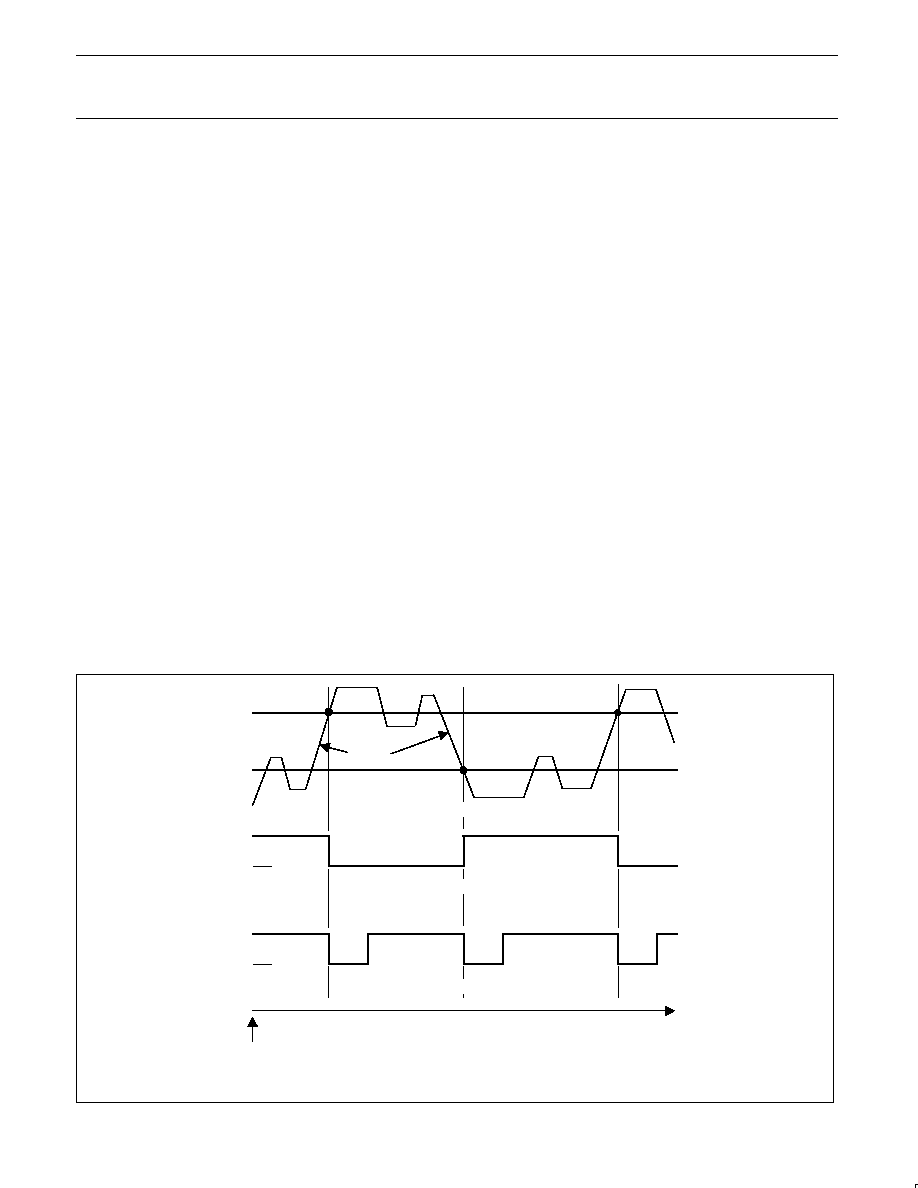
The OS response to the temperature is illustrated in Figure 5.
SL01392
Temp
*
*
*
POWER-UP
TIME
OS RESET
OS ACTIVE
OS OUTPUT IN INTERRUPT MODE
OS OUTPUT IN COMPARATOR MODE
OS RESET
OS ACTIVE
Tos
Thyst
READING TEMPERATURE & LIMITS
*
= OS is reset by either reading register or putting the device in shutdown.
Assumed that the fault queue is met at each Tos and Thyst crossing point.
Figure 5. OS response to temperature.
Philips Semiconductors
Product data sheet
LM75A
Digital temperature sensor and thermal Watchdog
TM
2004 Oct 05
8
I
2
C serial interface
The LM75A can be connected to a compatible 2-wire serial interface
I
2
C-bus as a slave device under the control of a controller or master
device, using two device terminals, SCL and SDA. The controller
must provide the SCL clock signal and write/read data to/from the
device through the SDA terminal. Notice that if the I
2
C common
pull-up resistors have not been installed as required for I
2
C-bus,
then an external pull-up resistor, about 10 k
, is needed for each of
these two terminals. The bus communication protocols are
described in the data communication section.
Slave address
The LM75A slave address on the I
2
C-bus is partially defined by the
logic applied to the device address pins A2, A1 and A0. Each of
them is typically connected either to GND for logic 0, or to V
CC
for
logic 1. These pins represent the three LSB bits of the device 7-bit
address. The other four MSB bits of the address data are preset to
`1001' by hard wiring inside the LM75A. Table 1 shows the device's
complete address and indicates that up to 8 devices can be
connected to the same bus without address conflict. Because the
input pins, SCL, SDA, A2A0, are not internally biased, it is
important that they should not be left floating in any application.
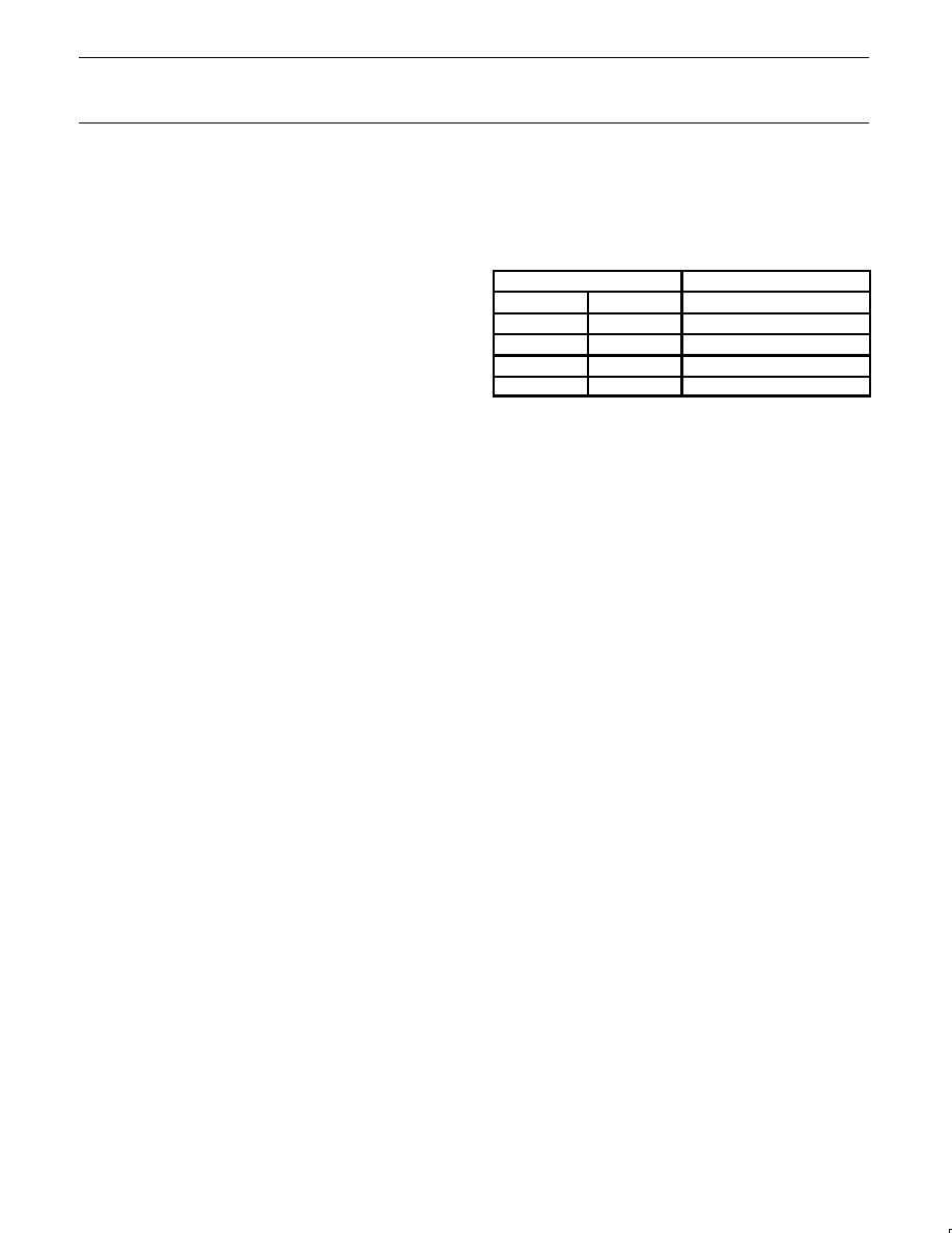
Table 1. Address table
1 = HIGH, 0 = LOW
MSB
LSB
1
0
0
1
A2
A1
A0
Register list
The LM75A contains four data registers beside the pointer register
as listed in Table 2. The pointer value, read/write capability and
default content at power up of the registers are also shown in the
Register table.
Table 2. Register table
Register name
Pointer value
R/W
POR state
Description
Conf
01H
R/W
00H
Configuration Register.
Contains a single 8-bit data byte. To set the device operating condition.
Default = 0.
Temp
00H
Read only
N/A
Temperature Register.
Contains two 8-bit data bytes. To store the measured Temp data.
Tos
03H
R/W
50 00H
Over-temp Shutdown threshold Register.
Contains two 8-bit data bytes. To store the over-temp shut-down Tos limit.
Default = 80
°
C.
Thyst
02H
R/W
4B 00H
Hysteresis Register.
Contains two 8-bit data bytes. To store the hysteresis Thyst limit.
Default = 75
°
C.
Pointer register
The pointer register contains an 8-bit data byte of which the two
LSB bits represent the pointer value of the other four registers, and
the other 6 MSB bits are equal to 0, as shown in the Pointer register
table (Table 3) and the Pointer value table (Table 4). The pointer
register is not accessible to the user, but is used to select the data
register for write/read operation by including the pointer data byte in
the bus command.
Table 3. Pointer register table
B7
B6
B5
B4
B3
B2
B1
B0
0
0
0
0
0
0
Pointer value
Table 4. Pointer value
B1
B0
Selected register
0
0
Temperature register (Temp)
0
1
Configuration register (Conf)
1
0
Hysteresis register (Thyst)
1
1
Overtemp shut-down register (Tos)
Because the Pointer value is latched into the Pointer register when
the bus command, which includes the pointer byte, is executed, a
read from the LM75A may or may not include the pointer byte in the
statement. To read again a register, which has been recently read
and the pointer has been preset, the pointer byte does not have to
be included. To read a register, which is different with the one that
has been recently read, the pointer byte must be included. However,
a write to the LM75A must always include the pointer byte in the
statement. The bus communication protocols are described in detail
in the data communication section.
At power-up, the Pointer value is equal to 0 and the Temp register is
selected; users can then read the Temp data without specifying the
pointer byte.
Philips Semiconductors
Product data sheet
LM75A
Digital temperature sensor and thermal Watchdog
TM
2004 Oct 05
9
Configuration register
The Configuration register is a write/read register and contains an 8-bit non-complement data byte that is used to configure the device for
different operation conditions. The Configuration register table (Table 5) shows the bit assignments of this register.
Table 5. Configuration register table
Bit
Name
R/W
POR
Description
B7B5
Reserved
R/W
000
Reserved for the manufacterer use.
B4B3
OS Fault queue
R/W
00
For OS Fault Queue programming.
Programmable queue data = 0, 1 ,2, 3 for queue value = 1, 2, 4, 6 respectively. Default = 0.
B2
OS Polarity
R/W
0
For OS Polarity selection.
1 = OS active HIGH, 0 = OS active LOW (default).
B1
OS Comp/Interrupt
R/W
0
For OS operation Mode selection.
1 = OS interrupt, 0 = OS comparator (default).
B0
Shut-down
R/W
0
For Device Operation Mode selection.
1 = Shut-down, 0 = Normal (default).
Temperature register (Temp)
The Temp register holds the digital result of temperature measurement or monitor at the end each A-to-D conversion. This register is read only
and contains two 8-bit data bytes consisting of one most significant (MS) data byte and one least significant (LS) data byte. However, only 11
bits of those two bytes are used to store the Temp data in 2's complement format with the resolution of 0.125
°
C. The Temp register table
(Table 6) shows the bit arrangement of the Temp data in the data bytes.
Table 6. Temp register table
Temp MS byte
Temp LS byte
MSB
LSB
MSB
LSB
B7
B6
B5
B4
B3
B2
B1
B0
B7
B6
B5
B4
B3
B2
B1
B0
Temp data (11 bits)
Not used
MSB
LSB
D10
D9
D8
D7
D6
D5
D4
D3
D2
D1
D0
X
X
X
X
X
Notice that when the Temp register is read, all 16 bits are provided to the bus and must be all collected by the controller to complete the bus
operation. However, only the 11 significant bits should be used, and the 5 LSB bits of the LS byte are zero and should be ignored. One of the
ways to calculate the Temp value in
°
C from the 11-bit Temp data is:
1. If the Temp data MSB bit D10 = 0 then the temperature is positive and
Temp value (
°
C) = + (Temp data) * 0.125
°
C
2. If the Temp data MSB bit D10 = 1 then the temperature is negative and
Temp value (
°
C) = (2's complement of Temp data) * 0.125
°
C
The Temp table (Table 7) shows examples of the Temp data and value.
Table 7. Temp table
Temp data
Temp value
11bit Binary (2's complement)
3-bit Hex
Decimal value
°
C
0111 1111 000
3F8h
1016
+127.000
°
C
0111 1110 111
3F7h
1015
+126.875
°
C
0111 1110 001
3F1h
1009
+126.125
°
C
0111 1101 000
3E8h
1000
+125.000
°
C
0001 1001 000
0C8h
200
+25.000
°
C
0000 0000 001
001h
1
+0.125
°
C
0000 0000 000
000h
0
0.000
°
C
1111 1111 111
7FFh
1
0.125
°
C
1110 0111 000
738h
200
25.000
°
C
11001001 001
649h
439
54.875
°
C
1100 1001 000
648h
440
55.000
°
C
Obviously, for 9-bit Temp data application in replacing the industry standard LM75, just use only 9 MSB bits of the two bytes and disregard
7 LSB bits of the LS byte. The 9-bit temp data with 0.5
°
C resolution of the LM75A is defined exactly in the same way as for the standard LM75
and it is here similar to the Tos and Thyst that is described next.
Philips Semiconductors
Product data sheet
LM75A
Digital temperature sensor and thermal Watchdog
TM
2004 Oct 05
10
Overtemp shut-down threshold (Tos) and hysteresis (Thyst) registers
These two registers are write/read registers, and also called set-point registers. They are used to store the user-defined temperature limits,
called overtemp shut-down threshold (Tos) and hysteresis (Thyst), for the device Watchdog operation. At the end of each conversion the Temp
data will be compared with the data stored in these two registers in order to set the state of the device OS output accordingly as described in the
"General operation" section.
Each of the set-point registers contains two 8-bit data bytes consisting of one MS data byte and one LS data byte the same as the Temp
register. However, only 9 bits of the two bytes are used to store the set-point data in 2's complement format with the resolution of 0.5
°
C. The
Tos register table (Table 8) and Thyst register table (Table 9) show the bit arrangement of the Tos data and Thyst data in the data bytes.
Notice that because only 9-bit data are used in the set-point registers, the device uses only the 9 MSB bits of the Temp data for data
comparison.
Table 8. Tos register table
Tos MS byte
Tos LS byte
MSB
LSB
MSB
LSB
B7
B6
B5
B4
B3
B2
B1
B0
B7
B6
B5
B4
B3
B2
B1
B0
Tos data (9 bits)
Not used
MSB
LSB
D8
D7
D6
D5
D4
D3
D2
D1
D0
X
X
X
X
X
X
X
Table 9. Thyst register table
Thyst MS byte
Thyst LS byte
MSB
LSB
MSB
LSB
B7
B6
B5
B4
B3
B2
B1
B0
B7
B6
B5
B4
B3
B2
B1
B0
Thyst data (9 bits)
Not used
MSB
LSB
D8
D7
D6
D5
D4
D3
D2
D1
D0
X
X
X
X
X
X
X
When a set-point register is read, all 16 bits are provided to the bus and must be collected by the controller to complete the bus operation.
However, only the 9 significant bits should be used and the 7 LSB bits of the LS byte are equal to zero and should be ignored.
The Tos and Thyst table (Table 10) shows examples of the limit data and value.
Table 10. Tos and Thyst table
Limit data
Limit temp value
11bit Binary (2's complement)
3-bit Hex
Decimal value
°
C
0111 1101 0
0FAh
250
+125.0
°
C
0001 1001 0
032h
50
+25.0
°
C
0000 0000 1
001h
1
+0.5
°
C
0000 0000 0
000h
0
0.0
°
C
1111 1111 1
1FFh
1
0.5
°
C
1110 0111 0
1CEh
50
25.0
°
C
1100 1001 0
192h
110
55.0
°
C
Philips Semiconductors
Product data sheet
LM75A
Digital temperature sensor and thermal Watchdog
TM
2004 Oct 05
11
OS output and polarity
The OS output is an open-drain output and its state represents
results of the device Watchdog operation as described in the
"General operation" section. In order to observe this output state, an
external pull-up resistor is needed. The resistor should be as large
as possible, up 200 k
, to minimize the temp reading error due to
internal heating by the high OS sinking current.
The OS output active state can be selected as HIGH or LOW by
programming bit B2 of the Configuration register: setting B2 to 1
selects OS active HIGH and setting B2 to 0 sets OS active LOW.
At power-up, this bit is equal to 0 and the OS active state is LOW.
OS comparator and interrupt modes
As described in the "General operation" section, the device OS
output responds to the result of the comparison between the Temp
data and the programmed limits, Tos and Thyst, in different ways
depending on the selected OS mode: OS comparator or OS
interrupt. The OS mode is selected by programming bit B1 of the
configuration register: setting B1 to 1 selects the OS interrupt mode,
and setting B1 to 0 selects the OS comparator mode. At power up,
this bit is equal to 0 and the OS comparator is selected.
The main difference between the two modes is that in OS
comparator mode, the OS output becomes active when the Temp
has exceeded the Tos and reset when the Temp has dropped below
the Thyst, reading a register or putting the device into shut-down
does not change the state of the OS output; while in OS interrupt
mode, once it has been activated either by exceeding the Tos or
dropping below the Thyst, the OS output will remain active
indefinitely until reading a register or putting the device into
shut-down occurs, then the OS output is reset.
The Tos & Thyst limits must be selected so that Tos temp value >
Thyst temp value. Otherwise, the OS output state will be undefined.
OS fault queue
Fault queue is defined as the number of faults that must occur
consecutively to activate the OS output. It is provided to avoid false
tripping due to noise. Because faults are determined at the end of
data conversions, fault queue is also defined as the number of
consecutive conversions returning a temperature trip. The value of
fault queue is selectable by programming the two bits B4 and B3 of
the configuration register. Notice that the programmed data and the
fault queue value are not the same. The Fault queue table (Table 11)
shows the one-to-one relationship between them. At power-up, fault
queue data = 0 and fault queue value = 1.
Table 11. Fault queue table
Fault queue data
Fault queue value
B4
B3
Decimal
0
0
1
0
1
2
1
0
4
1
1
6
Shutdown mode
The device operation mode is selected by programming bit B0 of the
Configuration register: Setting B0 to 1 will put the device into
shut-down mode. Resetting B0 to 0 for the device normal mode.
In shut-down mode, the device draws a small current of about
3.5
µ
A and the power dissipation is minimized; the temperature
conversion stops, but the I
2
C interface remains active and register
write/read operation can be performed. If the OS output is in
comparator mode, then it remains unchanged. Otherwise, the OS
output is reset in interrupt mode.
Power-up default and Power-on Reset
The LM75A always powers-up in its default state with:
Normal operation mode
OS comparator mode
Tos = 80
°
C
Thyst = 75
°
C
OS output active state = LOW
Pointer value = 0.
When the power supply voltage is dropped below the device
power-on reset level of about 1.9 V (POR) and then rises up again,
the device will be reset to its default condition as listed above.

Philips Semiconductors
Product data sheet
LM75A
Digital temperature sensor and thermal Watchdog
TM
2004 Oct 05
12
Data communication
The communication between the host and the LM75A must strictly
follow the rules as defined by the I
2
C-bus management. The
protocols for LM75A register read/write operations are illustrated by
the Figures as follows with these definitions:
1. Before a communication, the I
2
C-bus must be free or not busy. It
means that the SCL and SDA lines must be both released by all
devices on the bus, and they become HIGH by the bus pull-up
resistors.
2. The host must provide SCL clock pulses necessary for the
communication. Data is transferred in sequence of 9 SCL clock
pulses for every 8-bit data byte followed by 1-bit status of the
acknowledgement.
3. During data transfer, except the Start and Stop signals, the SDA
signal must be stable while the SCL signal is HIGH. It means
that SDA signal can be changed only during the LOW duration
of the SCL line.
4. S: Start signal, initiated by the host to start a communication,
the SDA goes from HIGH-to-LOW while the SCL is HIGH.
5. RS: Re-start signal, same as the Start signal, to start a read
command that follows a write command.
6. P: Stop signal, generated by the host to stop a communication,
the SDA goes from LOW-to-HIGH while the SCL is HIGH. The
bus becomes free thereafter.
7. W: Write bit, when the Write/Read bit = LOW in a write
command.
8. R: Read bit, when the Write/Read bit = HIGH in a read
command.
9. A: Device Acknowledge bit, returned by the LM75A. It is LOW if
the device works properly and HIGH if not. The host must
release the SDA line during this period in order to give the
device the control on the SDA line.
10. A
: Master Acknowledge bit, not returned by the device, but set
by the master or host in reading 2-byte data. During this clock
period, the host must set the SDA line to LOW in order to notice
the device that the first byte has been read for the device to
provide the second byte onto the bus.
11. NA: Not-Acknowledge bit. During this clock period, both the
device and host release the SDA line at the end of a data
transfer, the host is then enabled to generate the Stop signal.
12. In a write protocol, data is sent from the host to the device and
the host controls the SDA line, except during the clock period
when the device sends to the bus the device acknowledgement
signal.
13. In a read protocol, data is sent to the bus by the device and the
host must release the SDA line during the time that the device is
providing data onto the bus and controlling the SDA line, except
during the clock period when the master sends to the bus the
master acknowledgement signal.
Philips Semiconductors
Product data sheet
LM75A
Digital temperature sensor and thermal Watchdog
TM
2004 Oct 05
13
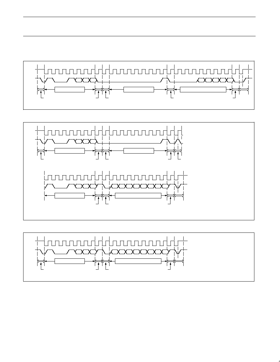
Protocols for writing and reading the registers
SL01393
1
2
3
4
5
6
7
8
9
1
2
3
4
5
6
7
8
9
1
2
3
4
5
6
7
8
9
1
0
0
1
A2
A1
A0
1
W
A
0
0
0
0
0
0
0
S
D4
D3
D2
D1
A
0
0
0
A
P
D0
DEVICE ADDRESS
POINTER BYTE
SCL
SDA
CONFIGURATION DATA BYTE
START
WRITE
DEVICE
ACKNOWLEDGE
DEVICE
ACKNOWLEDGE
STOP
DEVICE
ACKNOWLEDGE
Figure 6. Write configuration register (1-byte data).
SL01398
1
2
3
4
5
6
7
8
9
1
0
0
1
A2
A1
A0
R
A
DEVICE ADDRESS
SCL (cont.)
SDA (cont.)
READ
DEVICE
ACKNOWLEDGE
D4
D3
D2
D1
D0
D7
D6
D5
1
2
3
4
5
6
7
8
9
P
MASTER NOT
ACKNOWLEDGED
STOP
NA
DATA BYTE FROM DEVICE
1
2
3
4
5
6
7
8
9
1
2
3
4
5
6
7
8
9
1
0
0
1
A2
A1
A0
1
W
A
0
0
0
0
0
0
0
S
A
DEVICE ADDRESS
POINTER BYTE
SCL
SDA
START
WRITE
DEVICE
ACKNOWLEDGE
DEVICE
ACKNOWLEDGE
0
RE-START
RS
(next)
(next)
Figure 7. Read configuration register including Pointer byte (1-byte data).
SL01394
1
2
3
4
5
6
7
8
9
1
2
3
4
5
6
7
8
9
1
0
0
1
A2
A1
A0
R
A
S
D4
D3
D2
D1
NA
P
D0
DEVICE ADDRESS
SCL
SDA
DATA BYTE FROM DEVICE
START
READ
DEVICE
ACKNOWLEDGE
MASTER NOT
ACKNOWLEDGED
STOP
D7
D6
D5
Figure 8. Read configuration register with preset Pointer (1-byte data).
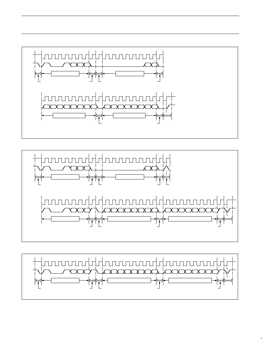
Philips Semiconductors
Product data sheet
LM75A
Digital temperature sensor and thermal Watchdog
TM
2004 Oct 05
14
SL01397
1
2
3
4
5
6
7
8
9
1
2
3
4
5
6
7
8
9
D7
D6
D5
D4
D3
D2
D1
A
D4
D3
D2
D1
A
D0
SCL (cont.)
SDA (cont.)
LS BYTE DATA
DEVICE
ACKNOWLEDGE
DEVICE
ACKNOWLEDGE
D7
D6
D5
P
STOP
1
2
3
4
5
6
7
8
9
1
2
3
4
5
6
7
8
9
1
0
0
1
A2
A1
A0
P0
W
A
0
0
0
0
0
0
P1
S
A
DEVICE ADDRESS
POINTER BYTE
SCL
SDA
START
WRITE
DEVICE
ACKNOWLEDGE
DEVICE
ACKNOWLEDGE
(next)
(next)
D0
MS BYTE DATA
Figure 9. Write Tos or Thyst register (2-byte data).
SL01396
1
2
3
4
5
6
7
8
9
1
2
3
4
5
6
7
8
9
1
0
0
1
A2
A1
A0
R
A
D4
D3
D2
D1
A
D0
DEVICE ADDRESS
SCL (cont.)
SDA (cont.)
MS BYTE FROM DEVICE
READ
DEVICE
ACKNOWLEDGE
MASTER
ACKNOWLEDGE
D7
D6
D5
D4
D3
D2
D1
D0
D7
D6
D5
1
2
3
4
5
6
7
8
9
P
MASTER NOT
ACKNOWLEDGED
STOP
NA
LS BYTE FROM DEVICE
1
2
3
4
5
6
7
8
9
1
2
3
4
5
6
7
8
9
1
0
0
1
A2
A1
A0
P0
W
A
0
0
0
0
0
0
P1
S
A
DEVICE ADDRESS
POINTER BYTE
SCL
SDA
START
WRITE
DEVICE
ACKNOWLEDGE
DEVICE
ACKNOWLEDGE
0
RE-START
RS
(next)
(next)
Figure 10. Read Temp or Tos or Thyst register including Pointer byte (2-byte data).
SL01395
1
2
3
4
5
6
7
8
9
1
2
3
4
5
6
7
8
9
1
0
0
1
A2
A1
A0
R
A
S
D4
D3
D2
D1
A
D0
DEVICE ADDRESS
SCL
SDA
MS BYTE FROM DEVICE
START
READ
DEVICE
ACKNOWLEDGE
MASTER
ACKNOWLEDGE
D7
D6
D5
D4
D3
D2
D1
D0
D7
D6
D5
1
2
3
4
5
6
7
8
9
P
MASTER NOT
ACKNOWLEDGED
STOP
NA
LS BYTE FROM DEVICE
Figure 11. Read Temp or Tos or Thyst register with preset Pointer (2-byte data).
Philips Semiconductors
Product data sheet
LM75A
Digital temperature sensor and thermal Watchdog
TM
2004 Oct 05
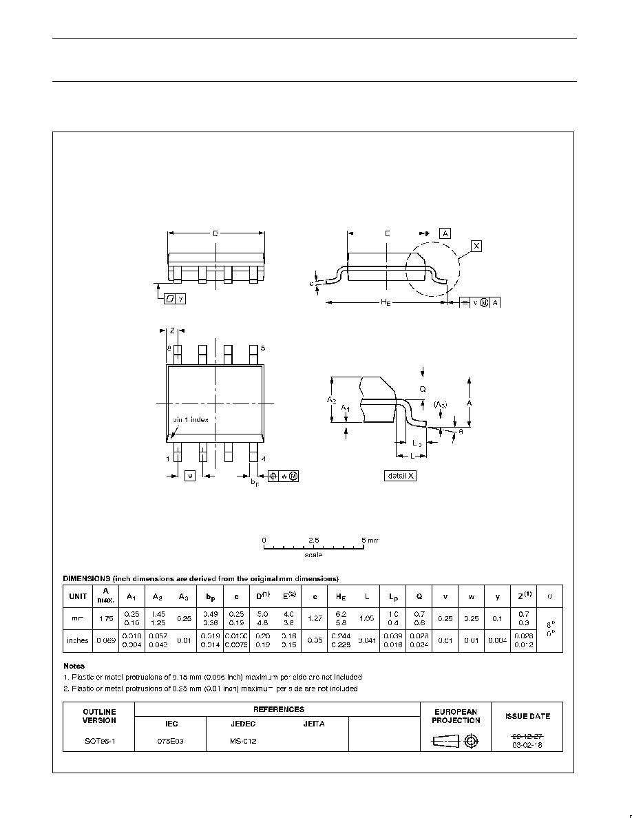
15
SO8:
plastic small outline package; 8 leads; body width 3.9 mm
SOT96-1

Philips Semiconductors
Product data sheet
LM75A
Digital temperature sensor and thermal Watchdog
TM
2004 Oct 05
16
TSSOP8:
plastic thin shrink small outline package; 8 leads; body width 3 mm
SOT505-1

Philips Semiconductors
Product data sheet
LM75A
Digital temperature sensor and thermal Watchdog
TM
2004 Oct 05
17
REVISION HISTORY
Rev
Date
Description
_2
20041005
Product data sheet (9397 750 14174). Supersedes data of 2001 Jul 16 (9397 750 08571).
Modifications:
·
"Features" section:
7
th
bullet: add "
±
3
°
C from 55
°
C to +125
°
C"
add "ESD" bullet
add "Latch-up" bullet
·
"Ordering information" table: `Topside mark' column
·
Figure 2, "Simplified block diagram" modified.
·
Section "Typical connection" re-named to "Typical application" (page 4); added resistor values to Figure 3.
_1
20010716
Product data (9397 750 08571). ECN 853-2266 26719 of 16 July 2001.

Philips Semiconductors
Product data sheet
LM75A
Digital temperature sensor and thermal Watchdog
TM
2004 Oct 05
18
Definitions
Short-form specification -- The data in a short-form specification is extracted from a full data sheet with the same type number and title. For detailed information see
the relevant data sheet or data handbook.
Limiting values definition -- Limiting values given are in accordance with the Absolute Maximum Rating System (IEC 60134). Stress above one or more of the limiting
values may cause permanent damage to the device. These are stress ratings only and operation of the device at these or at any other conditions above those given
in the Characteristics sections of the specification is not implied. Exposure to limiting values for extended periods may affect device reliability.
Application information -- Applications that are described herein for any of these products are for illustrative purposes only. Philips Semiconductors make no
representation or warranty that such applications will be suitable for the specified use without further testing or modification.
Disclaimers
Life support -- These products are not designed for use in life support appliances, devices, or systems where malfunction of these products can reasonably be
expected to result in personal injury. Philips Semiconductors customers using or selling these products for use in such applications do so at their own risk and agree
to fully indemnify Philips Semiconductors for any damages resulting from such application.
Right to make changes -- Philips Semiconductors reserves the right to make changes in the products--including circuits, standard cells, and/or software--described
or contained herein in order to improve design and/or performance. When the product is in full production (status `Production'), relevant changes will be communicated
via a Customer Product/Process Change Notification (CPCN). Philips Semiconductors assumes no responsibility or liability for the use of any of these products, conveys
no license or title under any patent, copyright, or mask work right to these products, and makes no representations or warranties that these products are free from patent,
copyright, or mask work right infringement, unless otherwise specified.
Contact information
For additional information please visit
http://www.semiconductors.philips.com.
Fax: +31 40 27 24825
For sales offices addresses send e-mail to:
sales.addresses@www.semiconductors.philips.com.
©
Koninklijke Philips Electronics N.V. 2004
All rights reserved. Published in the U.S.A.
Date of release: 10-04
Document number:
9397 750 14174
Philips
Semiconductors
Data sheet status
[1]
Objective data sheet
Preliminary data sheet
Product data sheet
Product
status
[2] [3]
Development
Qualification
Production
Definitions
This data sheet contains data from the objective specification for product development.
Philips Semiconductors reserves the right to change the specification in any manner without notice.
This data sheet contains data from the preliminary specification. Supplementary data will be published
at a later date. Philips Semiconductors reserves the right to change the specification without notice, in
order to improve the design and supply the best possible product.
This data sheet contains data from the product specification. Philips Semiconductors reserves the
right to make changes at any time in order to improve the design, manufacturing and supply. Relevant
changes will be communicated via a Customer Product/Process Change Notification (CPCN).
Data sheet status
[1] Please consult the most recently issued data sheet before initiating or completing a design.
[2] The product status of the device(s) described in this data sheet may have changed since this data sheet was published. The latest information is available on the Internet at URL
http://www.semiconductors.philips.com.
[3] For data sheets describing multiple type numbers, the highest-level product status determines the data sheet status.
Level
I
II
III
Document Outline
- GENERAL DESCRIPTION
- FEATURES
- APPLICATIONS
- ORDERING INFORMATION
- PINNING
- SIMPLIFIED BLOCK DIAGRAM
- TYPICAL APPLICATION
- ABSOLUTE MAXIMUM RATINGS 1
- OPERATING RATINGS
- DC ELECTRICAL CHARACTERISTICS
- I 2 C INTERFACE AC CHARACTERISTICS 1
- FUNCTIONAL DESCRIPTION
- PACKAGE OUTLINE
- REVISION HISTORY
- Data sheet status
- Definitions
- Disclaimers