LPC2210
16/32-bit ARM microcontroller;
with 10-bit ADC and external memory interface
Rev. 01 -- 09 February 2004
Preliminary data
1.
General description
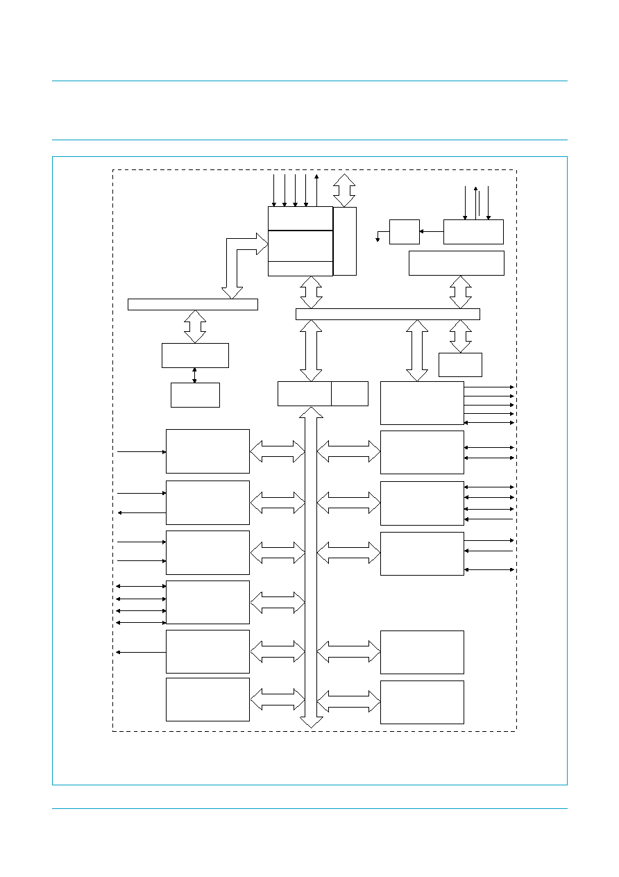
The LPC2210 is based on a 16/32 bit ARM7TDMI-STM CPU with real-time emulation
and embedded trace support. For critical code size applications, the alternative 16-bit
Thumb Mode reduces code by more than 30% with minimal performance penalty.
With its 144 pin package, low power consumption, various 32-bit timers, 8-channel
10-bit ADC, PWM channels and up to 9 external interrupt pins this microcontroller is
particularly suitable for industrial control, medical systems, access control and
point-of-sale. LPC2210 provides up to 76 GPIO depending on bus configuration. With
a wide range of serial communications interfaces, it is also very well suited for
communication gateways, protocol converters and embedded soft modems as well
as many other general-purpose applications.
2.
Features
2.1 Key features
s
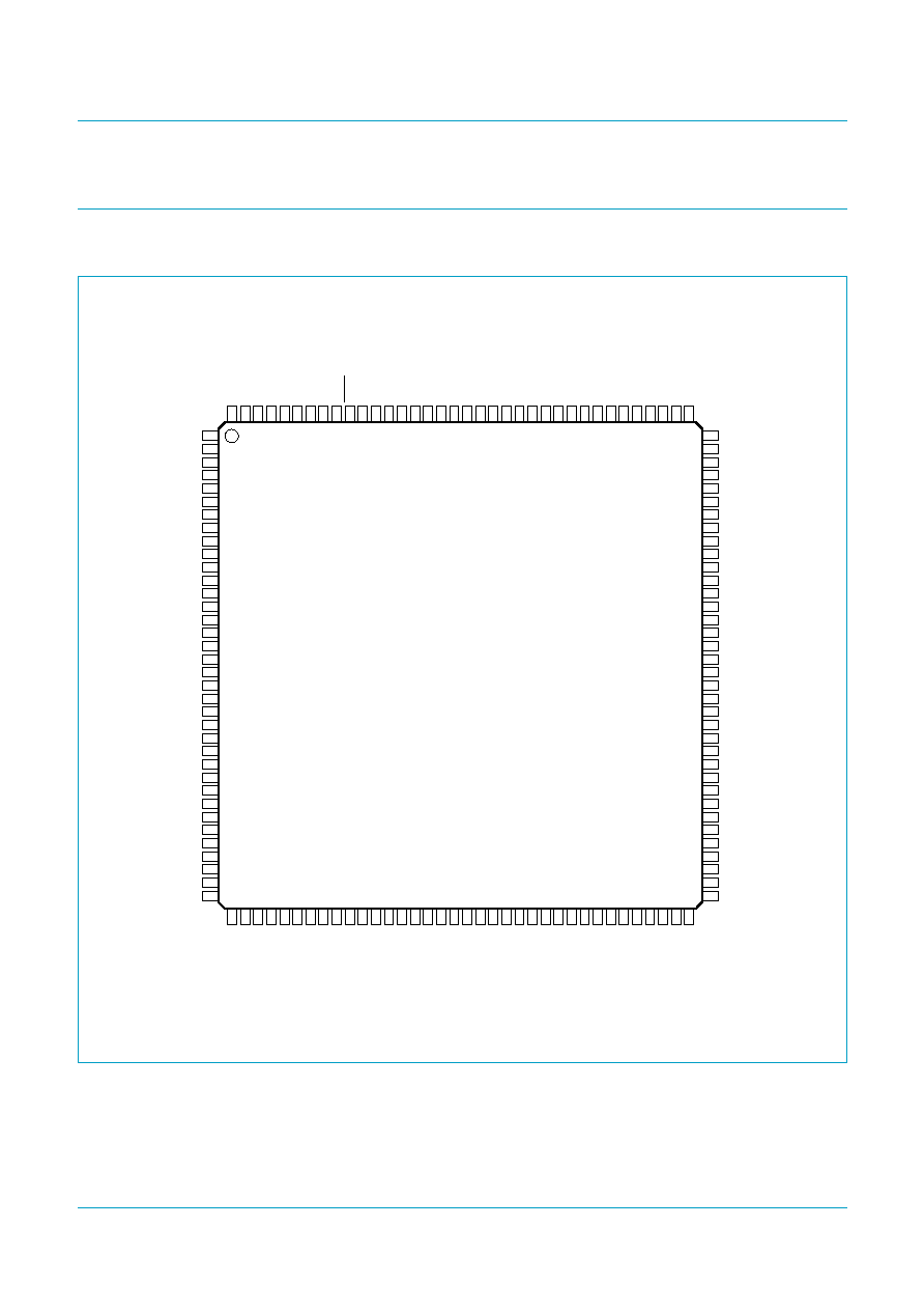
16/32-bit ARM7TDMI-S microcontroller in a LQFP144 package.
s
16 kB on-chip Static RAM.
s
Serial boot-loader using UART0 provides in-system download and programming
capabilities.
s
EmbeddedICE-RT and Embedded Trace interfaces offer real-time debugging with
the on-chip RealMonitor software as well as high speed real-time tracing of
instruction execution.
s
Eight channel 10-bit A/D converter with conversion time as low as 2.44
�
s.
s
Two 32-bit timers (with 4 capture and 4 compare channels), PWM unit (6 outputs),
Real Time Clock and Watchdog.
s
Multiple serial interfaces including two UARTs (16C550), Fast I
2
C (400 kbits/s)
and two SPIsTM.
s
Vectored Interrupt Controller with configurable priorities and vector addresses.
s
Configurable external memory interface with up to four banks, each up to 16 Mb
and 8/16/32 bit data width.
s
Up to 76 general purpose I/O pins (5 V tolerant). Up to 9 edge or level sensitive
external interrupt pins available.
Philips Semiconductors
LPC2210
16/32-bit ARM microcontrollers with external memory interface
Preliminary data
Rev. 01 -- 09 February 2004
2 of 39
9397 750 12872
� Koninklijke Philips Electronics N.V. 2004. All rights reserved.
s
60 MHz maximum CPU clock available from programmable on-chip
Phase-Locked Loop.
s
On-chip crystal oscillator with an operating range of 1 MHz to 30 MHz.
s
Two low power modes, Idle and Power-down.
s
Processor wake-up from Power-down mode via external interrupt.
s
Individual enable/disable of peripheral functions for power optimization.
s
Dual power supply:
x
CPU operating voltage range of 1.65 V to 1.95 V (1.8 V
�
0.15 V).
x
I/O power supply range of 3.0 V to 3.6 V (3.3 V
�
10%) with 5 V tolerant I/O
pads. 16/32-bit ARM7TDMI-S processor.
3.
Ordering information
3.1 Ordering options
Table 1:
Ordering information
Type number
Package
Name
Description
Version
LPC2210FBD144 LQFP144
plastic low-profile quad flat package, 144
leads, body 20
�
20
�
1.4 mm
SOT486-1
Table 2:
Part options
Type number
Flash memory
RAM
CAN
Temperature
range (
�
C)
LPC2210FBD144
-
16 kB
-
-
40 to +85

Philips Semiconductors
LPC2210
16/32-bit ARM microcontrollers with external memory interface
Preliminary data
Rev. 01 -- 09 February 2004
5 of 39
9397 750 12872
� Koninklijke Philips Electronics N.V. 2004. All rights reserved.
5.2 Pin description
Table 3:
Pin description
Symbol
Pin
Type
Description
P0.0 to P0.31
42, 49, 50,
58, 59, 61,
68, 69, 75,
76, 78,
83-85, 92,
99, 100, 101,
121-123, 4-6,
8, 21, 23, 25,
3, 2, 33
I/O
Port 0: Port 0 is a 32-bit bi-directional I/O port with individual direction
controls for each bit. The operation of port 0 pins depends upon the pin
function selected via the Pin Connect Block.
Pins 26 and 31 of port 0 are not available.
P0.0
42
O
TxD0 -- Transmitter output for UART0.
O
PWM1 -- Pulse Width Modulator output 1.
P0.1
49
I
RxD0 -- Receiver input for UART0.
O
PWM3 -- Pulse Width Modulator output 3.
I
EINT0 -- External interrupt 0 input
P0.2
50
I/O
SCL -- I
2
C clock input/output. Open drain output (for I
2
C compliance).
I
CAP0.0 -- Capture input for Timer0, channel 0.
P0.3
58
I/O
SDA -- I
2
C data input/output. Open drain output (for I
2
C compliance).
O
MAT0.0 -- Match output for Timer0, channel 0.
I
EINT1 -- External interrupt 1 input.
P0.4
59
I/O
SCK0 -- Serial clock for SPI0. SPI clock output from master or input to slave.
I
CAP0.1 -- Capture input for Timer0, channel 1.
P0.5
61
I/O
MISO0 -- Master In Slave OUT for SPI0. Data input to SPI master or data
output from SPI slave.
O
MAT0.1 -- Match output for Timer0, channel 1.
P0.6
68
I/O
MOSI0 -- Master Out Slave In for SPI0. Data output from SPI master or data
input to SPI slave.
I
CAP0.2 -- Capture input for Timer0, channel 2.
P0.7
69
I
SSEL0 -- Slave Select for SPI0. Selects the SPI interface as a slave.
O
PWM2 -- Pulse Width Modulator output 2.
I
EINT2 -- External interrupt 2 input.
P0.8
75
O
TxD1 -- Transmitter output for UART1.
O
PWM4 -- Pulse Width Modulator output 4.
P0.9
76
I
RxD1 -- Receiver input for UART1.
O
PWM6 -- Pulse Width Modulator output 6.
I
EINT3 -- External interrupt 3 input.
P0.10
78
O
RTS1 -- Request to Send output for UART1.
I
CAP1.0 -- Capture input for Timer1, channel 0.